Novram
Novram
Novram
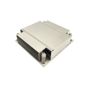
95W LGA115X 1U Server Radiator Air-cooled Radiator Computer Server Radiator
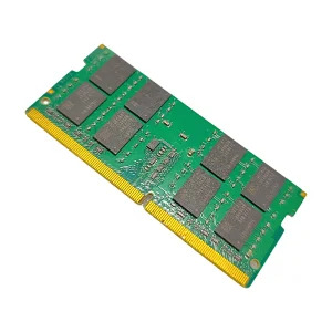
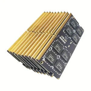
RAM DDR4 16GB 3200MHz Compatible with PC Computer Memory RAM 1600MHz 2666mHz 2400MHz 3200MHz
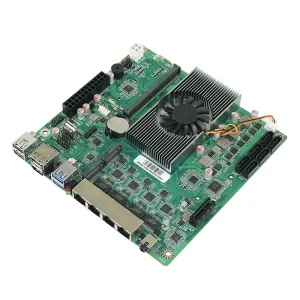
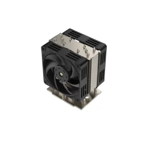
Computer Processor SP5 N97 Server Cooler Air-cooled Cooler CPU Cooler Dual Ball Bearings
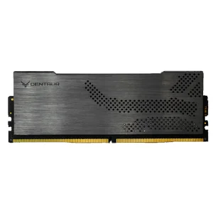
Desktop ECC DDR5 4GB RAM Memory Module 2133MHz/2400MHz/2666MHz/3200MHz/1333MHz in Stock
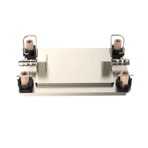
Igh Performance 1U Copper LGA4677 400W Water Cooler Block LGA4189 Liquid CPU Cooler Server Processor
The global transition from mercury-vapor lamps to solid-state disinfection has positioned UVC LED technology at the forefront of public health and industrial hygiene. Unlike conventional gas-discharge lighting, UVC LED modules operating within the critical 260nm to 280nm ultraviolet range offer instant-on operation, environmental compliance, and extreme design flexibility. However, harnessing this microbicidal potential demands deep electronics expertise and uncompromising thermal management.
Novram Electronics Co., Ltd. leverages its extensive background in high-performance electronics, SMT PCBA manufacturing, and thermal cooling solutions to build state-of-the-art UVC LED systems. By combining high-frequency circuit designs with custom heat-sink integration, we address the primary bottleneck of UVC semiconductors: thermal dissipation. As an established developer of complex server radiators and high-speed processing boards, our capabilities guarantee stable current regulation and optimal heat management—vital requirements for maximizing the operational lifespan of ultraviolet emitting diodes.
UVC LEDs typically convert only 2% to 5% of electrical energy into optical radiation; the remaining 95%+ is lost as heat. If the junction temperature of the LED chip rises beyond rated limits:
Our deep competence in SMT assembly and server-grade cooling systems ensures that every custom UVC LED module is designed from the substrate up to guarantee thermal protection.
From multi-wavelength arrays to tailored PCB sub-mounts, we build high-power modules matching exact OEM/ODM operational criteria.
We utilize Aluminum Nitride (AlN) direct copper-bonded substrates instead of standard FR4 or basic MCPCBs. This reduces thermal resistance (Rth-j) below 8 K/W, permitting higher drive currents and maximizing UV irradiance output.
Our modules feature selectable single or dual-wavelength bands. Typically configured at 265nm–275nm for rapid DNA/RNA destruction, we can integrate UVA/UVB channels (365nm–405nm) for secondary photocatalytic oxidation.
Choose from standard hemispherical quartz lenses providing 120° Lambertian emission profile or flat windows coupled with micro-reflector cavities to output highly collimated 60°/30° beams for deep target penetration.
| Module Specifications | Standard Configuration | High-Irradiance Custom Line | Key Operational Advantage |
|---|---|---|---|
| Peak Wavelength | 270nm - 275nm (UVC) | 260nm - 268nm / 365nm Dual-Band | Targeted viral/bacterial absorption peak |
| Substrate Material | MCPCB (Aluminum / Copper base) | Direct Plated Copper (DPC) on AlN Ceramic | Minimal thermal impedance, maximum lifetime |
| Optical Output (Po) | 20mW - 120mW per module | 350mW - 1200mW High-Power Arrays | High-throughput sterilization for flowing media |
| Input Voltage / Drive | DC 12V / 24V Constant Current | Integrated PWM Constant-Current Driver | Prevents thermal runaway and maintains output linearity |
| Optical Window | Quartz Glass Encapsulation | Hermetic Quartz Lens with Reflector | High UV transmittance (>90%) without degradation |
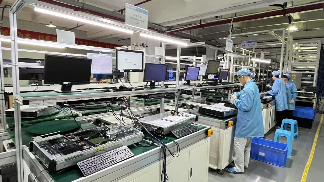
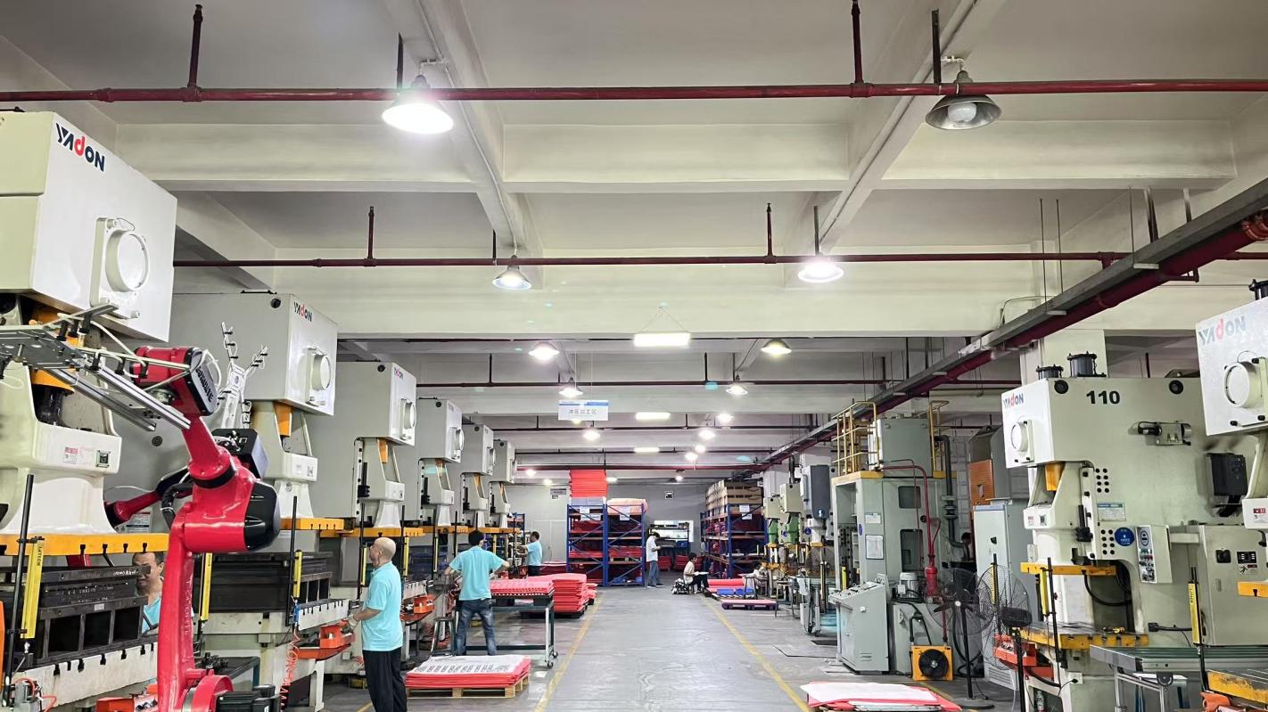
Operating from our modern 3,860㎡ facility in Shenzhen, we ensure continuous throughput, precision component sourcing, and extreme repeatability.
Shenzhen represents the absolute core of the global optoelectronics supply chain. Operating from our modern 3,860㎡ manufacturing facility, Novram Electronics integrates automated pick-and-place lines, nitrogen-reflow soldering ovens, and advanced automated optical inspection (AOI) systems. This advanced infrastructure allows us to mount delicate UVC chipsets without placing mechanical stress on the quartz domes.
By leveraging partnerships with over 860 qualified supply chain partners, we guarantee access to premium LED wafers, high-performance thermal adhesives, and raw materials even during market fluctuations. Our integrated vertical manufacturing covers everything from custom double-sided PCB fabrication, SMT assembly, wire bonding, to radiator attachment, reducing external lead times and maintaining stringent quality assurance.
Designed for seamless integration into diverse industrial, municipal, and consumer environments.
Designed for dynamic water purification units. Built-in high-performance thermal heat sinks dissipate energy directly into liquid lines or external heat pipes, supporting continuous operation without degrading disinfection rates.
Configured as high-density arrays for HVAC ductwork. These systems generate high UV-C irradiance to sterilize airborne pathogens in rapid airflow pathways. Enhanced with moisture-resistant conformal coatings.
Optimized for medical equipment, clinical automation, logistics belt sorting, and consumer appliances. Incorporates multi-wavelength arrays to address different types of biological contamination.
For industrial B2B buyers and system integrators, selecting a UVC module supplier involves assessing key technical factors:
Exporting to over 40 countries requires adapting to local electrical regulations and environmental safety standards. Novram Electronics supports global operations by offering comprehensive certification support, including CE, FCC, RoHS, and EPA registrations. We utilize hazardous-substance-free SMT processes, aligning with European green initiatives.
Every shipment is backed by documented performance characteristics. We provide optical simulation files, thermal resistance maps, and integration guidelines. Our 76-engineer R&D center is available to troubleshoot electrical, optical, or mechanical challenges during system integration.
How we are driving research to enhance Wall-Plug Efficiency (WPE) and build smart, IoT-enabled disinfection networks.
Current commercial UVC LEDs average a Wall-Plug Efficiency (WPE) of 3% to 6%. Our current research focuses on packaging optimization, specifically utilizing high-purity single-crystal sapphire bases and high-reflective internal coatings to boost light extraction efficiency by up to 25%. This allows systems to achieve equivalent germicidal output at lower driving currents, reducing thermal loads.
Next-generation disinfection modules will shift from passive emitters to smart, interactive sub-systems. We are actively developing modules featuring onboard optical sensors to monitor UV output in real time. These sensors automatically adjust power to compensate for natural LED degradation over time. Integrated I2C/Modbus communication protocols allow these modules to connect directly to industrial IoT control boards.
Combining UVC and UVA/UVB channels allows for comprehensive sanitization processes. While UVC damages the DNA/RNA structures of pathogens, UVA activates photocatalytic titanium dioxide (TiO2) coatings to oxidize volatile organic compounds. By producing these multi-wavelength modules on a single ceramic board, we help customers save space and simplify their system architecture.
Answers to key engineering and procurement questions for international B2B buyers.
How does Novram Electronics manage heat dissipation in its high-power UVC LED modules?
We address thermal dissipation at three levels. First, we use Aluminum Nitride (AlN) substrates, which offer high thermal conductivity (>170 W/mK). Second, we design customized copper-core or water-cooled heatsinks specifically for high-power arrays. Third, our SMT lines use high-purity solder with minimal voiding to reduce interfacial thermal resistance between the LED pad and the PCB.
What testing procedures do the modules undergo before export?
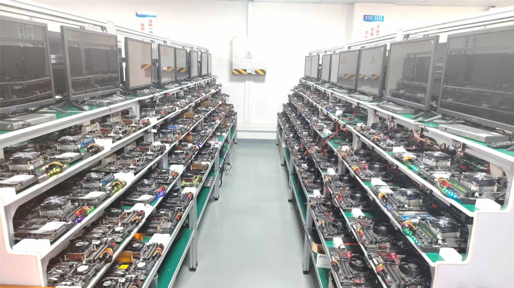
Every module undergoes 100% functional, optical, and thermal testing before shipment. This includes checking forward voltage stability, testing peak wavelength alignment via spectrometer analysis, and conducting burn-in tests to identify infant mortality. Our 42 professional QC inspectors monitor every step of production.
Can Novram customize PCB dimensions and driver specifications?
Yes. We specialize in OEM and ODM customization. We can adjust the board dimensions, electrical inputs (e.g., constant voltage DC 12V/24V or constant current), array patterns, output power, and optical window materials to fit your specific housing and integration constraints.
What is the typical lifespan (L70) of your UVC LED modules under constant operation?
Under rated driving current and with junction temperatures maintained below 60°C, our premium UVC modules achieve an L70 lifetime of more than 10,000 to 15,000 hours. We provide thermal design assistance to help you maintain optimal operating temperatures in your end products.
How does your SMT PCBA experience benefit B2B buyers of custom assemblies?
Our 9 years of SMT PCBA experience allows us to manufacture complex control circuitry alongside UVC LEDs. This means we can integrate power converters, sensor inputs, delay timers, and status indicators onto a single, space-saving board, reducing assembly steps and wiring points for our customers.
What are your typical OEM/ODM sample and mass production lead times?
Standard prototype samples are typically delivered within 7 to 10 working days. For custom OEM designs requiring layout modifications and custom heat sink designs, lead times average 2 to 3 weeks. Mass production orders are typically dispatched within 25 to 35 days, depending on component availability and order volume.
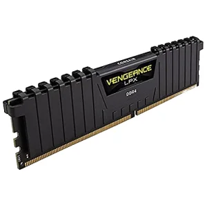
Best Price Desktop Memory Ram Ddr4 8GB 2400MHz Ram Computer Memory Module Ddr4 8GB
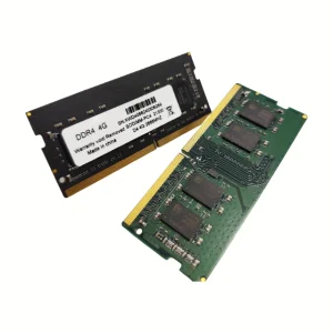
LAPTOP Computer Gaming Memory RAM DDR4 4GB 2666MHz Laptop Memory Card DDR4 8GB 3200MHz
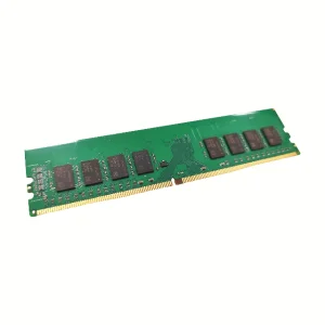
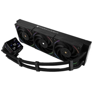
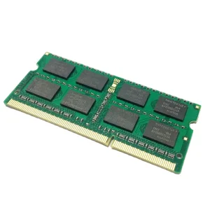
Hot Sale Memory RAM DDR4 4GB 8GB 16GB 2666MHz 3200MHz for Laptop and Desktop Computer Pc NB
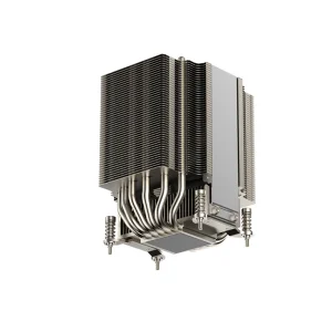
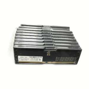
Computer Server Memory DDR5 32GB 5600MHz Desktop Memory Module RAM 14800MHz 5600MHz 6000MHz
A look inside our modern facility, showcasing our production lines and quality inspection systems.