Novram
Novram
Novram
Explore our industrial-grade multi-layer circuit designs, advanced power supplies, and high-performance memory modules.
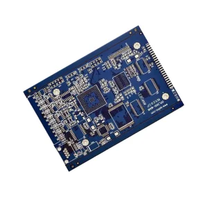
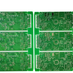
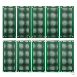
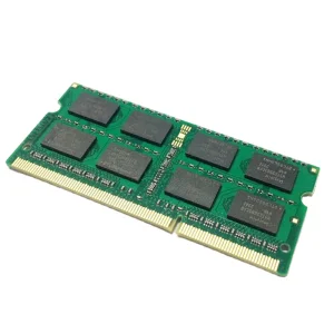
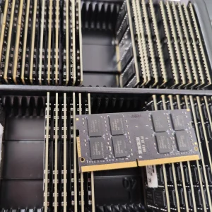
In the high-stakes arena of industrial hardware, choosing a qualified PCB supplier and exporter is no longer just about hunting for the lowest unit cost. It is a critical optimization problem spanning signal integrity, layer-stack thermal dissipation, raw material traceability, and compliance with strict standards like ISO9001 and UL.
Modern electrical engineering teams face a two-front challenge. On one side, they must integrate high-speed digital technologies (like DDR5 DRAM interfaces running at 6400 MT/s and above) while keeping EMI emissions under control. On the other side, global sourcing managers must shield their operations from supply chain delays, unpredictable freight logistics, and raw material volatility (such as fluctuating copper, glass fiber, and epoxy resin costs).
This report details the exact processes, engineering rules, and geographic benefits that allow advanced tier-1 PCB plants in China to deliver prototype designs in 24 hours while keeping mass production runs efficient, reliable, and fully compliant with international markets.
Even minor errors in dielectric constant (Dk) consistency across multilayer boards can degrade signal paths, resulting in data loss. Our partner fabrication units use high-grade KB-6160 glass fiber bases and premium FR4 substrates to ensure stability under demanding thermal loads.
How localized component clusters and state-of-the-art SMT capabilities yield unmatched speed and cost advantages.
Shenzhen provides instant access to raw substrates (FR4, Rogers, Megtron), copper clad laminates (CCL), photoresists, and active IC components. This keeps transport times low and protects production timelines from localized material shortages.
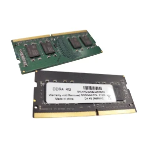
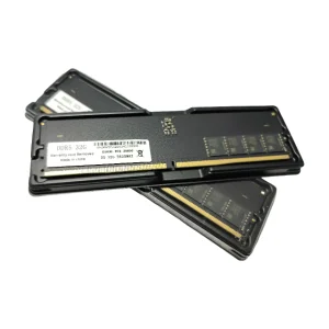
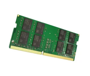
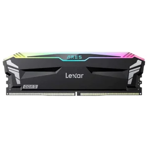
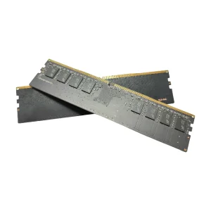
By coupling custom PCB printing with our core SMT assembly lines, we install BGA, QFN, and passive packages seamlessly. This direct integration is key when mounting high-speed DDR4/DDR5 memory modules onto custom industrial boards.
Located near major commercial hubs, we process shipping customs quickly. This ensures that double-sided PCBs, complex multilayer boards, and assembled memory components reach customers across more than 40 countries on schedule.
Novram Electronics Co., Ltd. is a professional DRAM and storage solution provider, alongside high-performance PCBA and PCB design processing. Established in 2016 in Shenzhen, China, we have developed a comprehensive platform that supports global OEMs, ODMs, and industrial electronics clients.
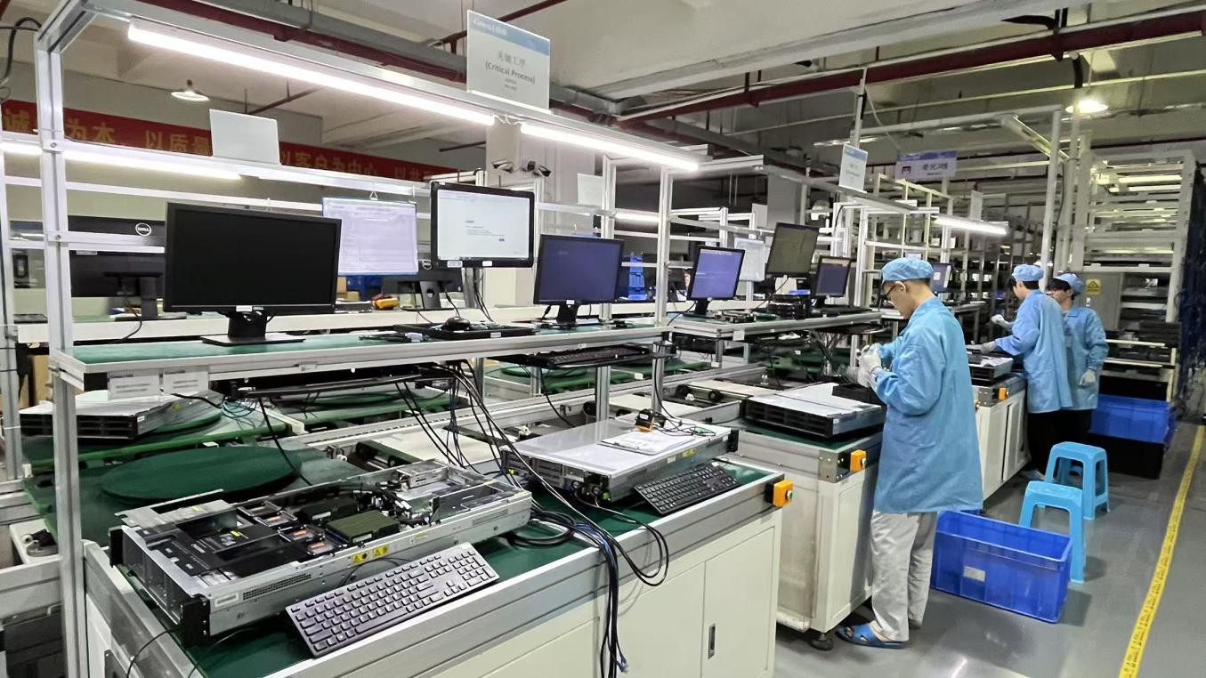
Operating a modern, state-of-the-art 3,860㎡ manufacturing facility, Novram combines advanced high-precision SMT pick-and-place lines, lead-free soldering machinery, and rigorous quality inspection rigs. With over 9 years of industry experience and 7 years of export expertise, we deliver custom circuit assemblies and high-speed memory systems to clients across 40+ countries.
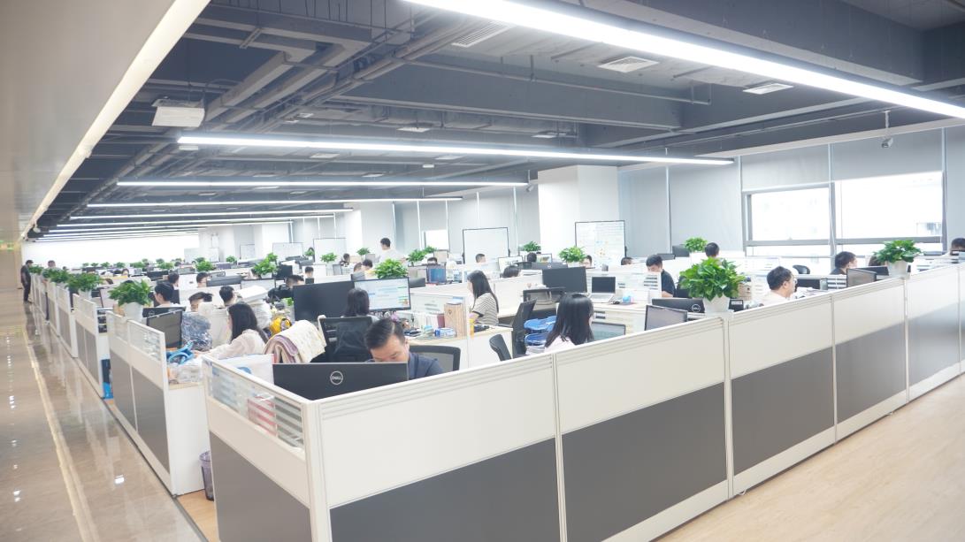
Our commitment to reliable, high-yield manufacturing is backed by our intensive quality processes. We maintain a staff of 42 professional quality inspectors who oversee validation protocols, while our 76-member engineering R&D team introduces roughly 138 new designs annually to keep pace with changing market demands.
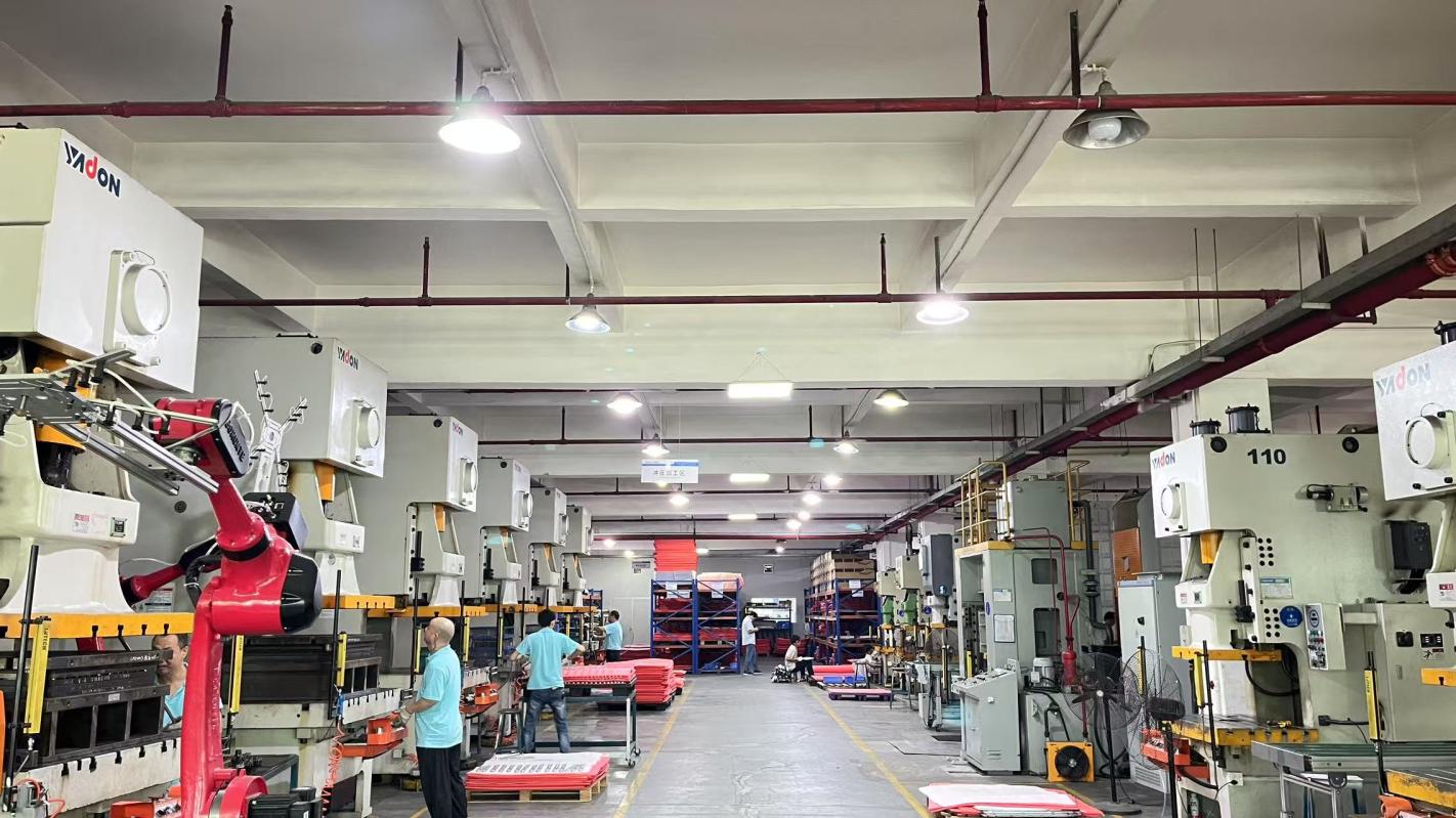
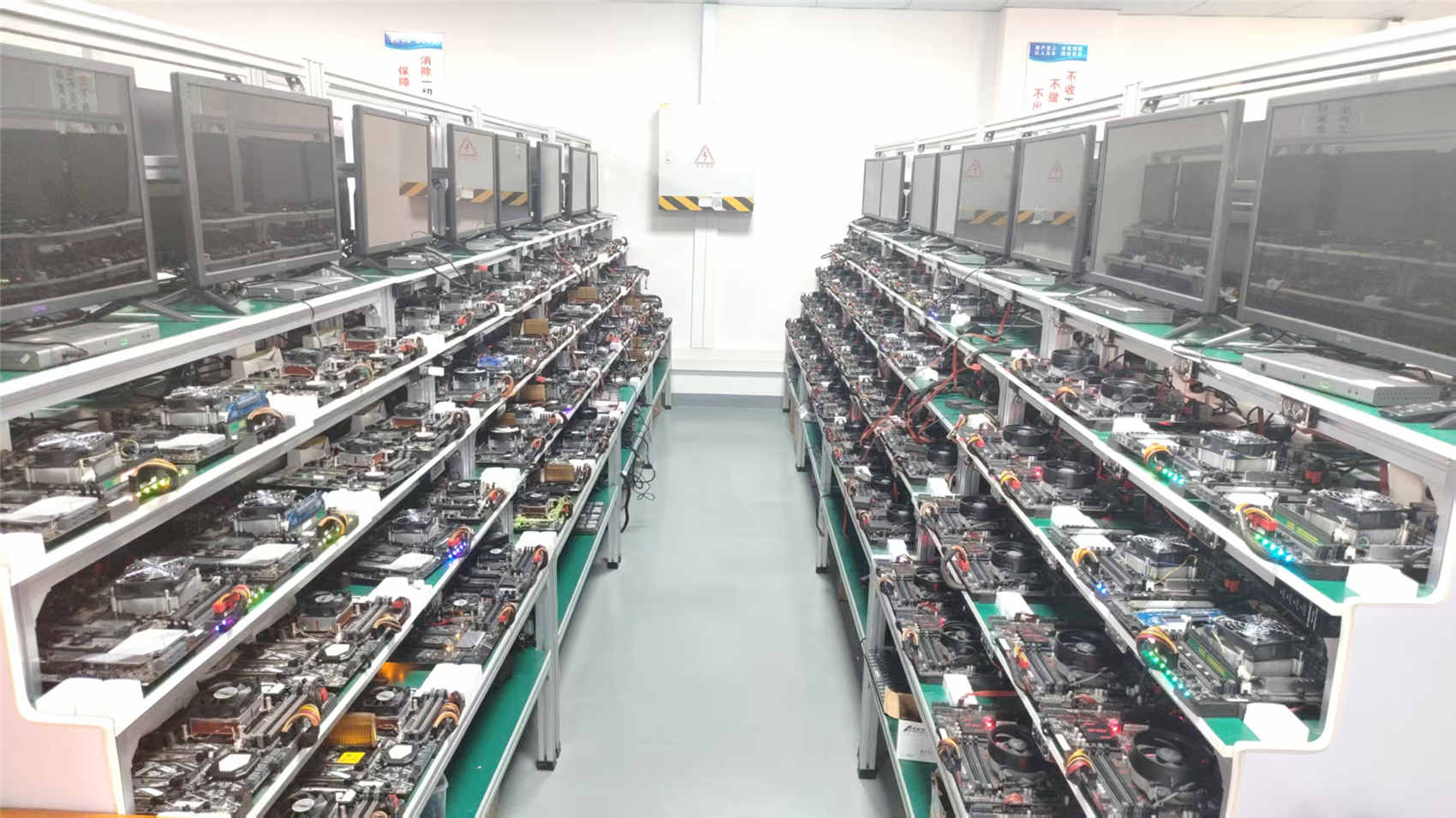
From single-layer HASL prototypes to complex 32-layer Immersion Silver boards, we meet demanding electrical specifications.
A reliable board design relies on selecting the right copper thickness, substrate material, and surface finish. As an experienced exporter, we align with IPC-A-610 Class 2 and Class 3 manufacturing standards to ensure long-term field reliability.
Our collaborative factories support standard and advanced design rules to handle complex electronic layouts:
| Technical Parameter | Standard Capability | Advanced Capability |
|---|---|---|
| Layer Count Range | 1 to 8 Layers | Up to 32 Layers / Rigid-Flex |
| Minimum Line Width/Spacing | 4 mil / 4 mil | 3 mil / 3 mil (HDI) |
| Dielectric Substrates | FR4 (TG130 - TG170) | High TG (TG180), Halogen-Free, Rogers |
| Impedance Tolerance | ±10% | ±5% (Precision Differential Control) |
| Aspect Ratio | 8:1 | 12:1 |
Strategic answers to compliance, tariff management, and international engineering support.
Navigating global compliance rules is a core requirement for electronics exporters. We ensure that our materials and manufacturing processes comply with international standards, helping our customers pass regulatory audits without issues.
To guard against material and shipping delays, we rely on established partnerships and robust risk-management strategies:
Tailored production methods designed for diverse operating environments.
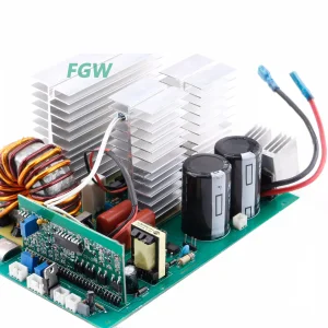
Our heavy-copper, multi-layer designs provide the reliable current carrying capacity needed for motor controllers, power supply motherboards, and welding equipment control circuits. These layouts are built to run continuously in demanding, high-noise industrial environments.
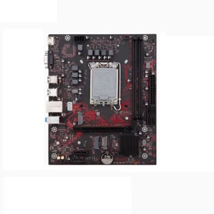
Featuring low-loss substrates and precision differential pair impedance control, our boards support the clean signals and data integrity required by DDR5 memory architectures and high-density, multi-port motherboards.
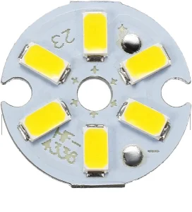
We supply high-thermal-conductivity metal-core PCBs (MCPCBs) and lightweight FR4 layouts for bright LED arrays and smart household appliances, balancing efficient heat dissipation with competitive manufacturing costs.
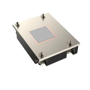
High-speed, high-density system boards generate substantial heat. By combining copper-based server heatsinks with high-speed memory modules, we deliver complete thermal solutions for demanding server architectures.
Our components are built to handle high frequencies, protecting system stability and preventing thermal throttling in enterprise hardware deployments.
Modern layouts require close alignment between the active board layers, passive filters, and storage chips. We help engineering teams navigate these design variables through clear support at every stage:
Direct technical and logistical answers for B2B electronics buyers.
Browse our selection of specialized fabrication systems, heavy-duty welding controllers, and enterprise-class DRAM hardware.