Novram
Novram
Novram
In the rapidly changing electronics industry, the role of a PCBA (Printed Circuit Board Assembly) manufacturer has evolved from simple contract assembly factories to strategic co-development partners. Modern consumer hardware, advanced server platforms, and automotive networks demand robust assembly capabilities capable of handling sub-millimeter component tolerances, multi-layer high-density layouts, and high-frequency signal integrity.
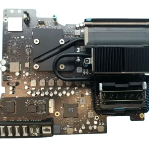
As semiconductors transition to denser architectures (such as FinFET, chiplets, and highly integrated System-on-Chips like the N100 or Core architectures), the underlying printed circuit board must serve as a reliable platform. A high-performance logic board or computer motherboard requires precise solder deposition, accurate pick-and-place component positioning, and controlled reflow thermal profiling. Even minor imperfections in solder viscosity, component positioning, or thermal cycles can result in micro-cracks, voiding, or signal degradation, causing failures in critical field applications.
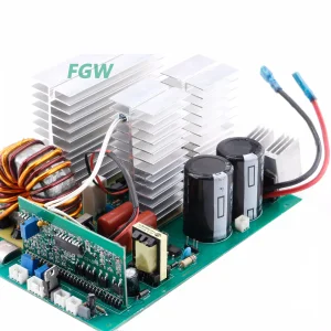
Industrial machinery, such as inverter welding units (e.g., ZX7-200/250 and ZX7-315 series), runs under continuous high temperatures and electrical stress. Factories must ensure robust copper trace thicknesses, thermal dissipation paths, and protective conformal coatings to prevent short-circuits in dusty, harsh environments.
Enterprise hardware requires advanced board design with composite structures (like copper-aluminum composites) and multi-channel memory layouts (DDR4/DDR5). Ensuring low signal attenuation at high bus speeds requires PCBA factories to utilize advanced signal-integrity validation and impedance-controlled assembly lines.
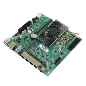
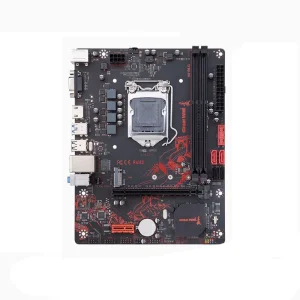
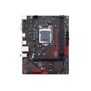
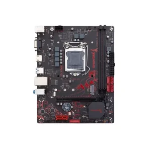
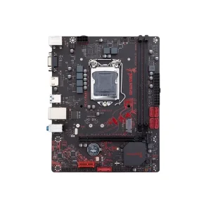
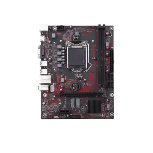
With the rise of edge computing, compact motherboard form factors like Mini-ITX (utilizing N100 or H510M platforms) must balance component density with thermal efficiency. Precision SMD placement and automated optical inspection are essential to build high-yield, compact logic systems.
Established in 2016 in the global electronics capital of Shenzhen, China, Novram Electronics Co., Ltd. is a high-technology manufacturer focused on the development, assembly, and testing of high-performance DRAM solutions and specialized PCBA modules. With 9 years of industry experience and 7 years of export experience, we deliver custom-engineered hardware to partners across more than 40 countries, yielding an annual export revenue of approximately US$18.6 million.
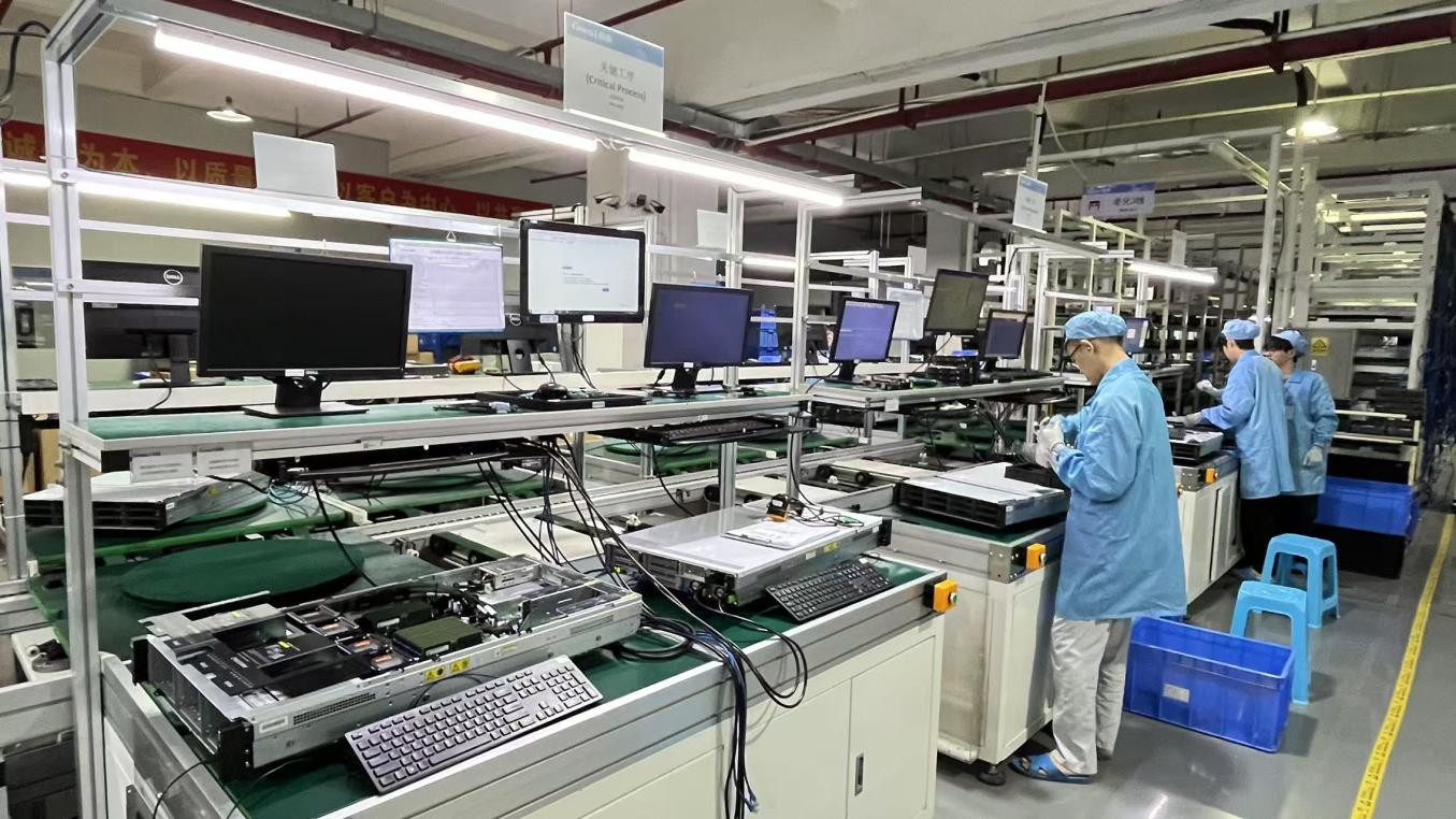
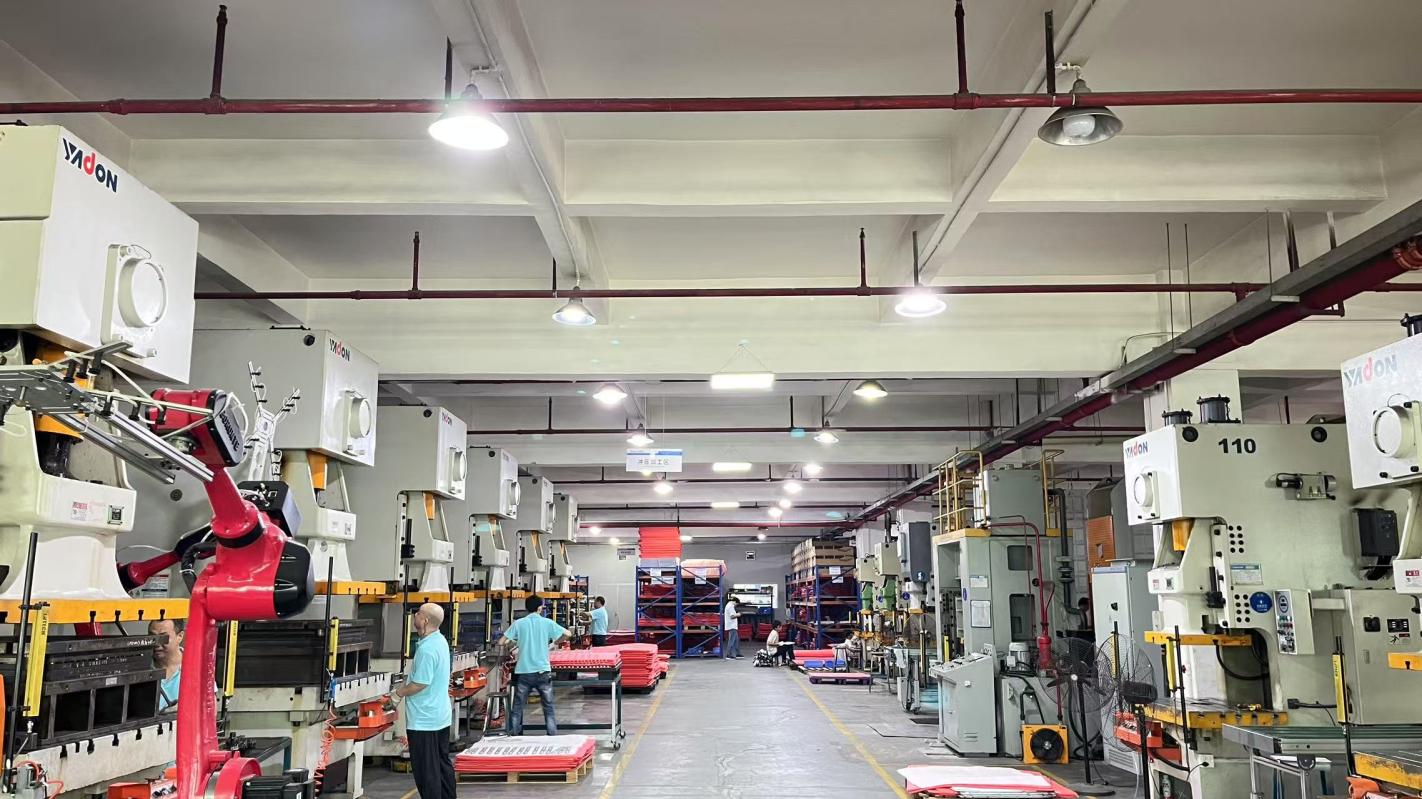
Our state-of-the-art 3,860㎡ manufacturing facility houses automated surface mount technology (SMT) lines, nitrogen reflow ovens, automated optical inspection (AOI) systems, and multi-stage testing setups. While specializing in DDR5 and legacy memory module packaging, Novram also provides OEM and ODM services for system integrators, embedded hardware projects, and industrial computing clients.
Our agility is supported by robust supply chains, comprising over 860 qualified supply chain partners. This network allows Novram to source high-grade original chipsets, passive components, and multilayer PCBs efficiently, even during periods of global component shortages.
Modern manufacturing in China has moved beyond labor-intensive assembly to integrated Industry 4.0 automation. For global system integrators and computer OEM brands, partnering with a Chinese PCBA manufacturer offers advantages in vertical integration. Sourcing channels in the Shenzhen region provide instant access to circuit materials, active components, custom passive arrays, connector systems, and structural cooling designs.
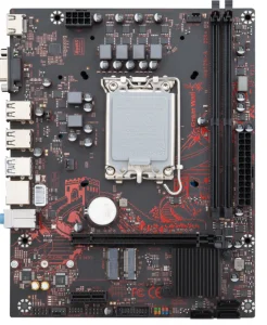
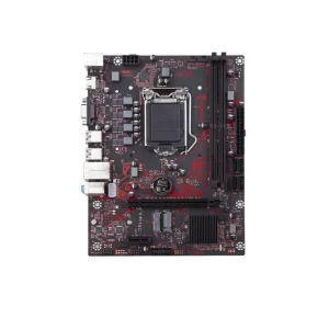
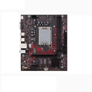
This clustering reduces material logistics turnaround from weeks to days. When an OEM requires complex boards, such as the LGA1700 H610 Chipset Motherboard or customized B760M-G Gaming PCBA platforms, engineering files can be updated, prototype bare PCBs fabricated, materials kitted, and SMT setups configured within a tight timeframe.
At Novram Electronics Co., Ltd., we combine this regional agility with modern tracking systems. Our supply chain utilizes real-time component validation to authenticate and inspect active elements before they reach the assembly lines. This localized control minimizes the risk of counterfeits and ensures that high-speed interfaces like DDR4 and DDR5 run within standard parameters.
With direct access to over 860 qualified supply chain partners, we secure core components (ICs, chipsets, capacitors) with short lead times, stabilizing output even during volatile market fluctuations.
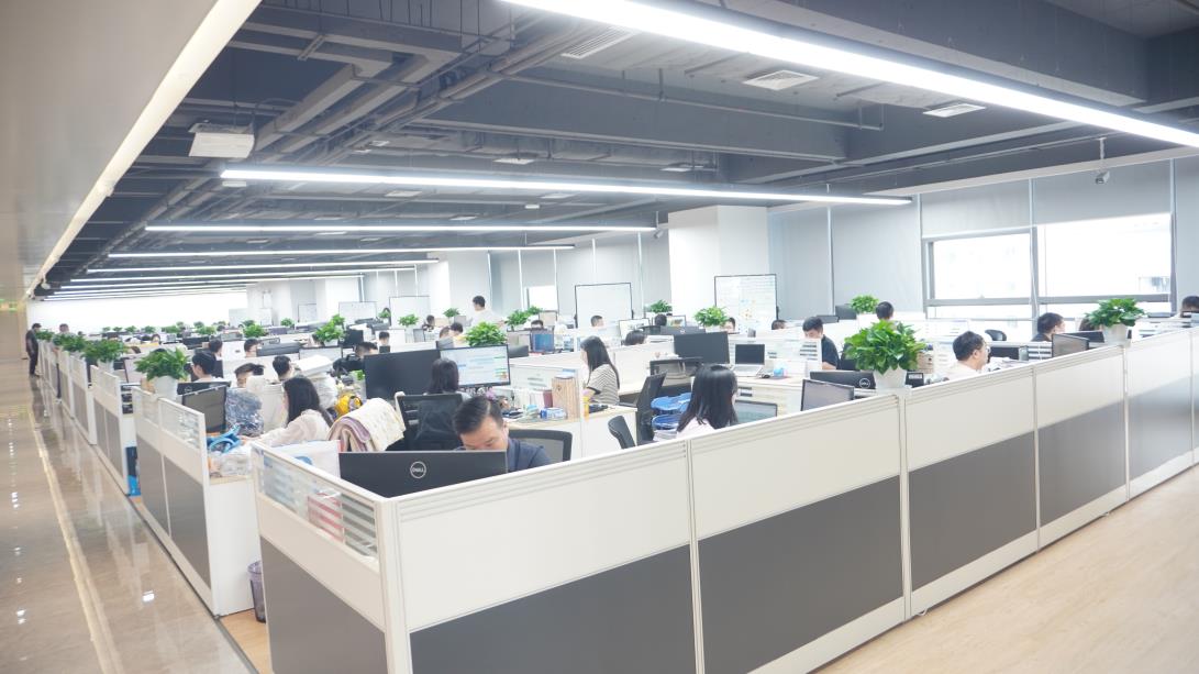
Our New Product Introduction (NPI) framework allows our 76 R&D engineers to translate Gerber files and BOM structures into production-ready assemblies quickly, accelerating your time-to-market.
We operate fully automated high-speed SMT systems, precision solder paste printers, inline 3D SPI (Solder Paste Inspection), and multi-zone convection reflow ovens to maintain product yields.
In electronics assembly, reliability is verified through consistent testing. Novram Electronics Co., Ltd. applies standard quality control across all production runs. Our quality control department is staffed by 42 dedicated inspectors who monitor assembly lines using automated, optical, and functional testing methods.
Every batch of memory modules and motherboards undergoes a strict multi-tier testing sequence to ensure durability under thermal stress, mechanical vibration, and continuous electrical loads:
Before component placement, 3D Solder Paste Inspection systems analyze the volume, height, alignment, and area of the printed paste on the pads. This step helps prevent solder opens, shorts, and voiding defects.
High-speed pick-and-place systems mount passive devices and micro-BGAs down to 0201 dimensions. Our multi-zone convection reflow ovens maintain precise thermal profiles, mitigating thermal stress and warp.
Inline AOI systems scan every circuit board post-reflow, detecting placement errors, missing components, polarity reversals, and bridged solder joints.
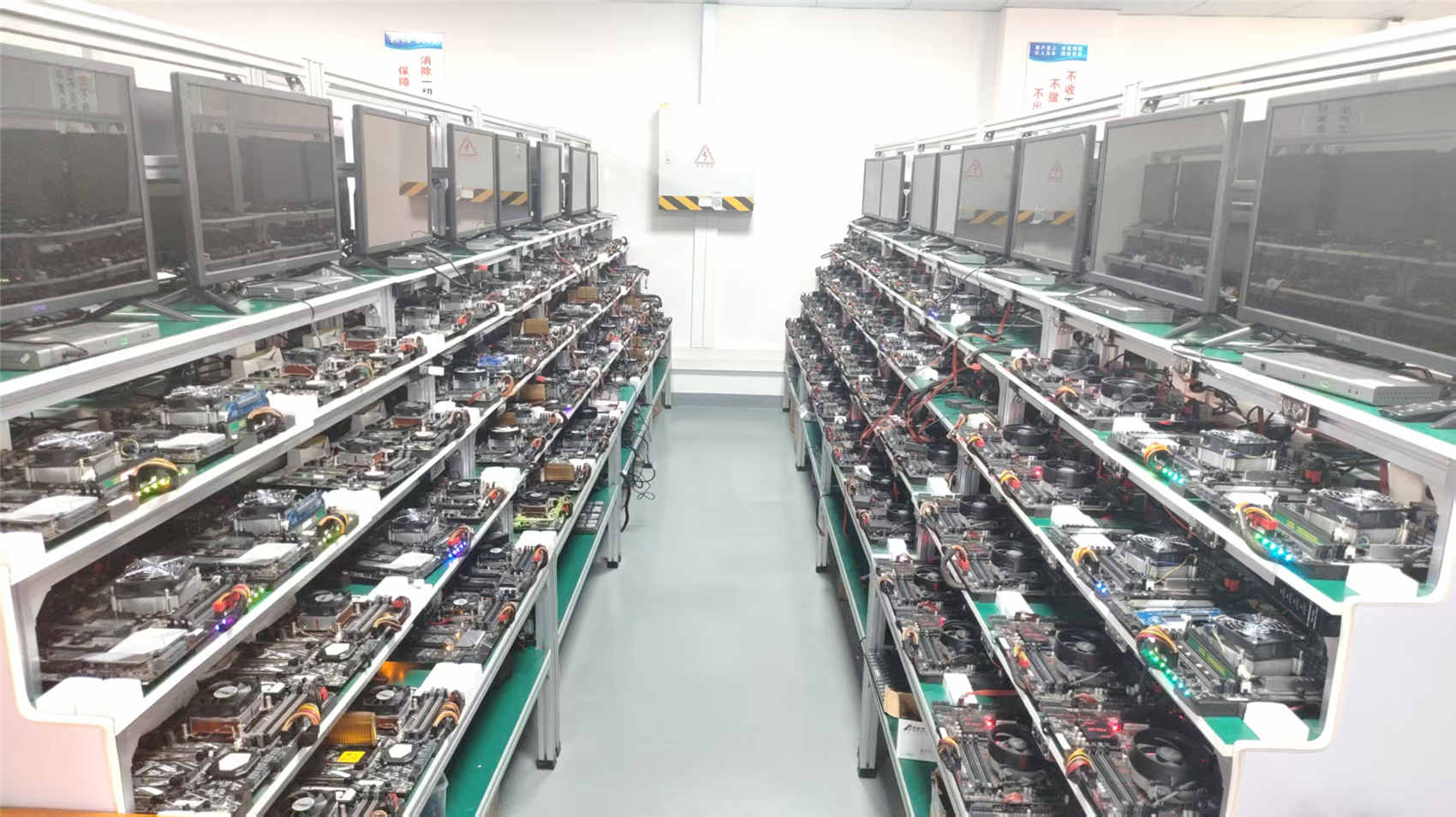
Assembled systems undergo functional validation. For computer motherboards, this includes testing CPU sockets, memory channels (DDR4/DDR5), PCI slots, and I/O hubs under full operating conditions.
Hardware designed for high-availability environments undergoes thermal chamber burn-in testing. Operating the boards at elevated temperatures helps identify potential early component failures, ensuring field reliability.
Advanced PCBA designs are integrated into multiple commercial, industrial, and consumer markets worldwide. From desktop motherboards in corporate environments to heavy-duty industrial control boards, electronic reliability directly influences operational runtime and equipment lifespans.
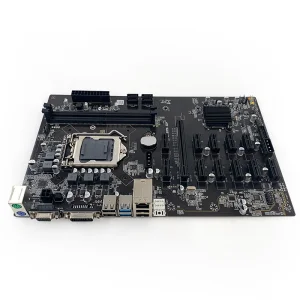
Reliable motherboard assemblies (such as the H81M-G or B250 series) provide stability for everyday office applications. Our focus on clean power delivery through VRM arrays minimizes hardware failures and system instability, helping enterprise fleets remain online without unexpected interruptions.
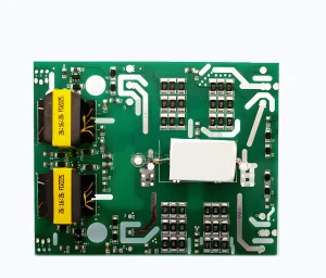
Heavy machinery, including high-power inverter welding systems like the ZX7-315, requires robust control and driver PCBA designs. Our assemblies feature reinforced circuit copper weight, high-temperature components, and isolating conformal coatings. These details protect the boards from dust, metallic particles, and thermal stress.
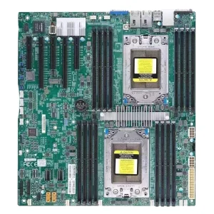
High-performance dual-channel server boards (e.g., Ultra Micro H11DSI-NT platform layouts) require optimized signal routing and low impedance levels. Novram's high-speed memory modules complement these server architectures, providing fast read-write speeds and data integrity for cloud service platforms and databases.
As the electronics industry transitions toward artificial intelligence, high-frequency IoT devices, and electric vehicles, printed circuit boards must adapt to handle faster signal transmission and increased component densities. Designers face the challenge of routing high-speed memory buses (like DDR5 and upcoming DDR6 systems) while preventing electromagnetic interference (EMI) and maintaining thermal stability.
Several key trends are defining the future of PCBA manufacturing:
Novram Electronics Co., Ltd. addresses these challenges by continuously updating our automated SMT lines. Our 76 R&D engineers work directly with customers to optimize trace impedance, design thermal management layouts, and select materials that balance cost, reliability, and regulatory compliance.