Novram
Novram
Novram
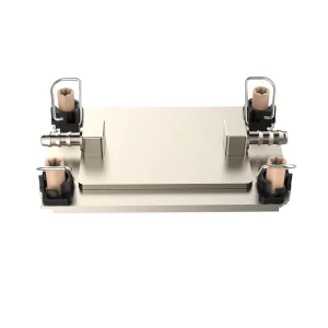
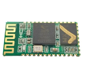
High-precision double/single-sided PCBs, customized modules, high-frequency substrates, and computing control platforms optimized for complex hardware deployments.
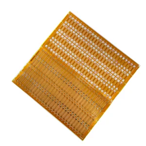
Decoding the foundational layer of modern electronics: why single and double-sided boards remain critical amidst rapid semiconductor scale-ups.
The global printed circuit board (PCB) sector continues to act as the foundational substrate of the digital age. While multi-layer and high-density interconnect (HDI) boards dominate consumer smartphones and cloud computing systems, single-sided and double-sided PCBs remain the primary structural backbone for a vast range of commercial, industrial, automotive, and consumer applications. Over 45% of the total hardware volume manufactured globally utilizes these standard topologies due to their superior cost-efficiency, direct routing capabilities, and robust thermal dynamics.
Single-sided printed circuit boards offer a single conductive copper layer laminated to a non-conductive substrate. They represent the optimal choice for cost-sensitive, high-volume production cycles like linear power supplies, LED drivers, baseline sensor packages, and consumer home appliances. In contrast, double-sided PCBs feature conductive traces on both sides, interconnected via Plated Through-Hole (PTH) technology. This structural evolution permits tighter component density, facilitates cross-routing on alternating layers, and accommodates more complex integrated circuits (ICs) while maintaining minimal production foot-prints.
Our global engineering networks dictate that successful product design hinges on selecting the exact material properties. Single and double-sided boards offer predictable electrical paths, lower parasitics, and ease of automated Optical Inspection (AOI). For high-frequency layouts, double-sided PCBs allow designers to utilize the bottom layer as a continuous ground plane, dramatically reducing electromagnetic interference (EMI) and cross-talk.
Detailed comparison of mechanical specifications, standard stackups, and material performance bounds.
| Feature Parameter | Single-Sided PCBs | Double-Sided PCBs | Primary Industrial Applications |
|---|---|---|---|
| Typical Substrate Materials | FR-1, FR-2, CEM-1, Aluminum, FR-4 | FR-4 High Tg, Aluminum, Polyimide, Taconic | Consumer controls, Automotive sensors, RF modules |
| Interconnection Type | Direct surface mounting only (SMT) | Plated Through-Hole (PTH), Via-in-Pad | Telecom infrastructure, high-power converters |
| Copper Weight Options | 0.5 oz to 2.0 oz | 0.5 oz to 6.0 oz (Heavy Copper) | Power supply units, motor controllers, EV chargers |
| Layer Count / Complexity | 1 Layer - Low routing complexity | 2 Layers - Medium to high density routing | Industrial computers, keyboard controllers, memory modules |
| Typical Lead Finish | HASL Lead-Free, OSP | ENIG, HASL, Immersion Silver/Gold | Precision sensors, military avionics, RF amplifiers |
By grouping component suppliers, raw laminate suppliers, and automated assembly (SMT) lines within a 10km radius, Shenzhen electronics manufacturers drastically reduce supply chain delays. Turnaround times for double-sided prototypes routinely drop to 24–48 hours, enabling rapid product iterations for global OEM/ODM brands.
Why do global electronic manufacturing services (EMS) partners continuously route their PCB production to specialized Chinese facilities? The answer lies in localized supply-chain vertical integration. Chinese factories in major industrial clusters (like Shenzhen and Guangdong) maintain direct physical access to primary raw materials—specifically high-grade copper-clad laminates (CCL), epoxy resins, dry films, and process chemicals.
This geographic integration eliminates cross-border logistics bottlenecks at the primary material level. Advanced tooling facilities feature fully automated CNC drilling centers, automated plating lines, and high-yield laser direct imaging (LDI) systems. Together, these systems maximize panel utilization rates and maintain rigid quality controls under IPC-A-600 Class 2 and Class 3 manufacturing paradigms.
Matching chemical physical properties with specialized operational environments to ensure system longevity.
Engineered with a thin, thermally conductive dielectric layer bonded between raw copper foil and a metal support plate. Crucial for solid-state lighting (LEDs), automotive headlights, power converters, and high-frequency cooling setups.
Standard flame-retardant (FR-4) woven glass reinforced epoxy resins. High Glass Transition temperature (Tg 170-180°C) substrates preserve dimensional stability, structural integrity, and trace tracking during high-temperature SMT lead-free reflow cycles.
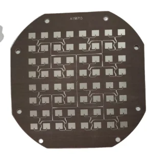
Ultra-low loss PTFE ceramic-filled materials (e.g., Taconic TLY-5) designed for high-frequency RF applications. These substrates guarantee stable dielectric constants (Dk) and low dissipation factors (Df) up to 10 GHz and beyond.
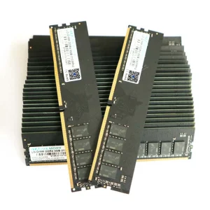
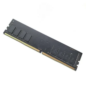
A premier global developer of high-performance DRAM memory, custom PCBs, and cooling solutions serving industrial OEM and ODM customers worldwide.
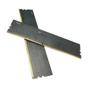
Novram Electronics Co., Ltd. is a professional DDR5 memory manufacturer based in Shenzhen, China, dedicated to delivering high-performance DRAM solutions for global OEM, ODM, and industrial customers. Established in 2016, the company has grown into a reliable supplier of DDR5 memory modules, serving partners across consumer electronics, industrial automation, embedded systems, gaming, and enterprise computing.
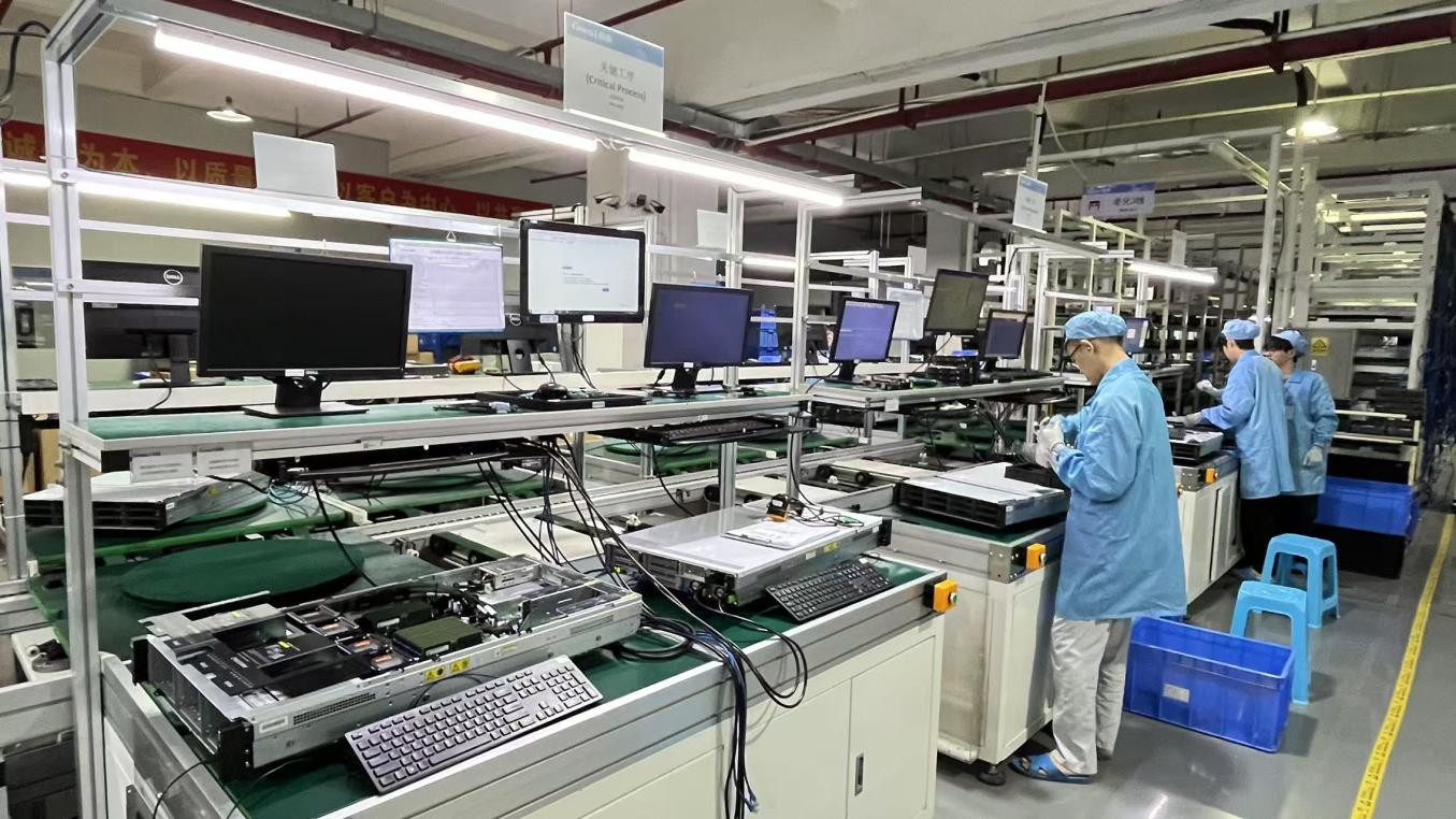
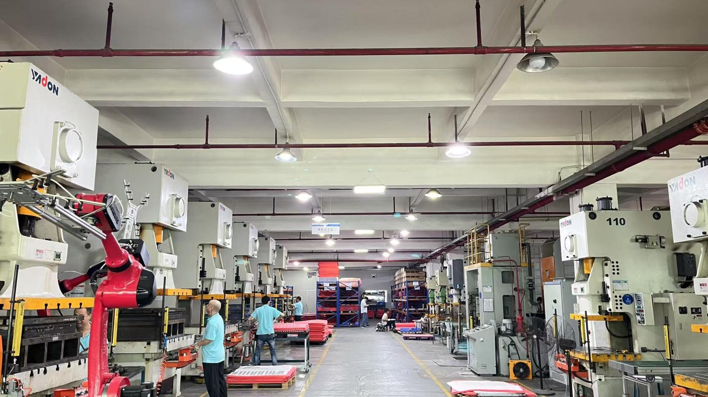
Operating from a modern 3,860㎡ manufacturing facility, Novram integrates advanced production equipment, strict quality management, and continuous R&D innovation to ensure every memory module meets international performance and reliability standards. Our experienced engineering team focuses on developing high-speed, stable, and energy-efficient DDR5 products for diverse computing applications.
With 9 years of industry experience and 7 years of export experience, Novram exports products to customers in more than 40 countries. The company achieves an annual export revenue of approximately US$18.6 million, supported by an efficient global supply chain and responsive customer service.
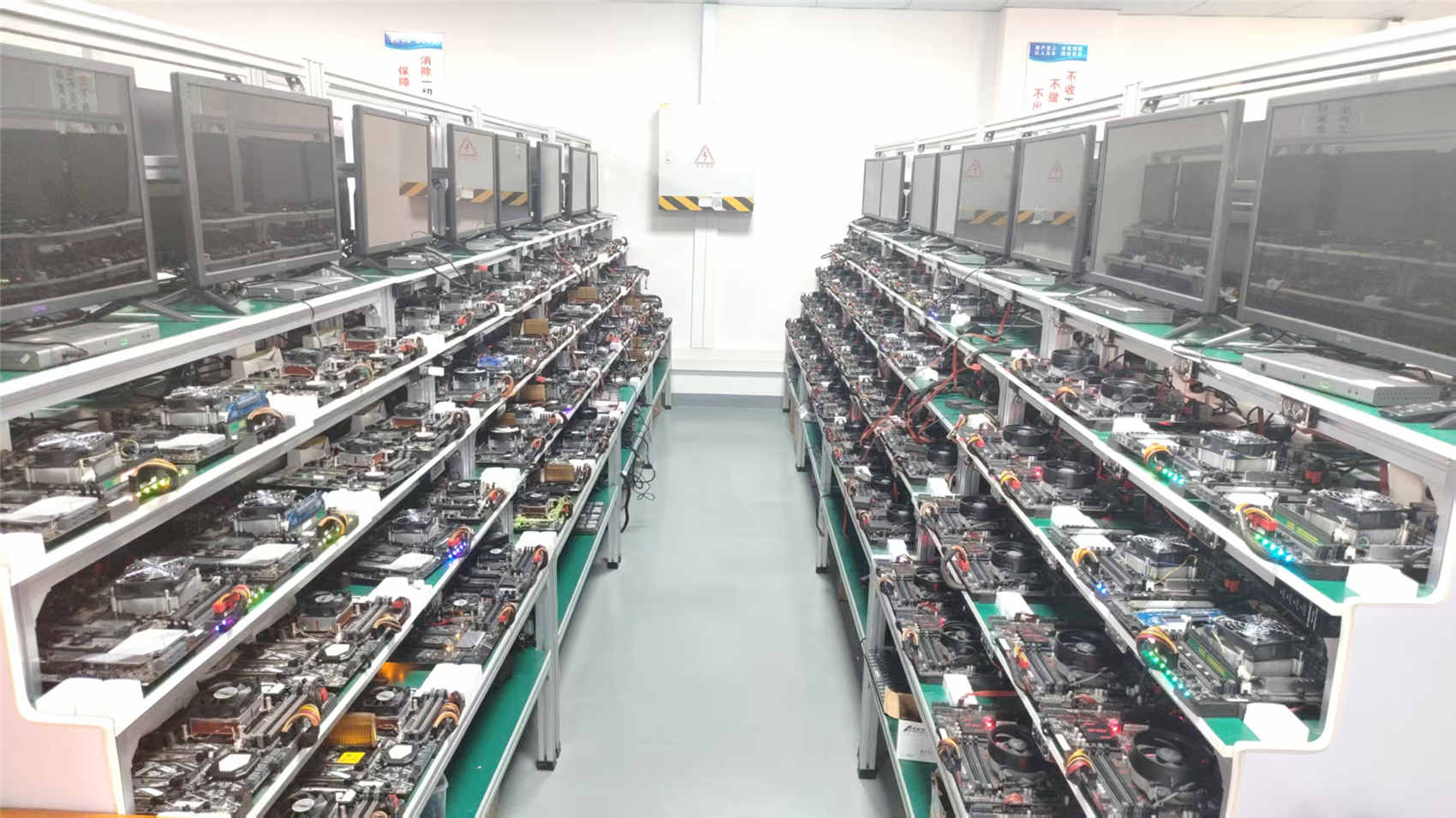
Quality is at the core of everything we do. Every DDR5 memory module undergoes 100% functional testing, compatibility testing, burn-in testing, temperature testing, and aging verification before shipment. Our quality control department consists of 42 professional inspectors, ensuring consistent product performance and long-term reliability.
Novram maintains strong partnerships with over 860 qualified supply chain partners, enabling stable production capacity and reliable component sourcing. Our primary customers include memory module brands, computer manufacturers, industrial PC companies, system integrators, distributors, wholesalers, and OEM/ODM partners worldwide.
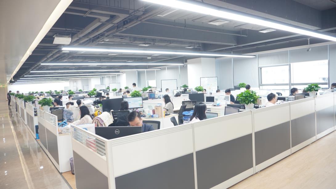
Innovation drives our competitiveness. Our dedicated R&D center is staffed by 76 experienced engineers, allowing us to introduce approximately 138 new products each year. We provide comprehensive OEM, ODM, private label, logo printing, packaging customization, capacity customization, firmware optimization, and product specification customization to meet different market requirements.
Today, Novram continues to invest in advanced manufacturing technologies, strict quality assurance, and customer-focused innovation. Our mission is to become a trusted global partner for high-performance DDR5 memory solutions by delivering reliable products, flexible customization, competitive pricing, and professional technical support.
Best practices for international sourcing teams to minimize defect rates and secure consistent shipping pipelines.
Ensure that your supplier executes an extensive Design for Manufacturability (DFM) verification prior to tooling. This resolves potential layout errors like insufficient copper-to-edge clearances, trace-width bottlenecks, and acid traps.
Specify the testing requirements in your RFQ docs: Flying Probe test or fixture-based electrical testing (E-test) is mandatory. Ask for Automated Optical Inspection (AOI) reports to identify minor solder mask or etching flaws before packing.
Single and double-sided PCBs are highly sensitive to ambient humidity. Demanded high-grade vacuum packaging with internal desiccant packs and humidity indicator cards. This prevents delamination during long ocean shipping runs.
Answering the most critical engineering and supply-chain questions faced by electronics procurement directors.
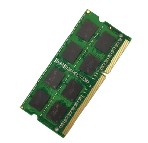
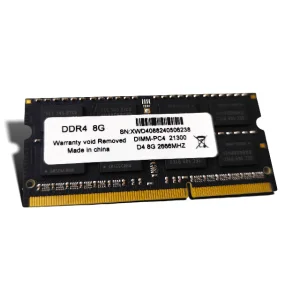
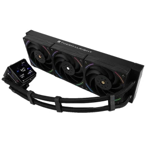
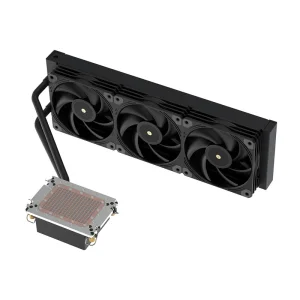
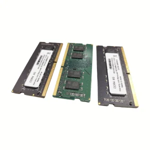
High-performance desktop/laptop memory, server thermal control fans, water blocks, and key board component systems.