Novram
Novram
Novram
Engineering reliability at the board level. These premium, multilayer electronics assemblies are optimized for American aerospace, telecommunications, and industrial automation standards.
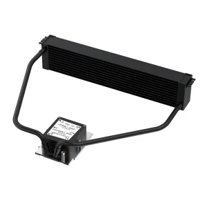
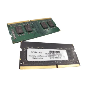
The United States electronics design sector is undergoing a massive transformation. Driven by initiatives like the CHIPS and Science Act and the rapid advancement of Artificial Intelligence (AI) compute architecture, the demand for complex multi-layer printed circuit boards (PCBs) is at an all-time high. Modern tech hubs across Silicon Valley, Austin, Boston, and the defense clusters of Virginia require boards that can manage extremely dense routing, high data transmission speeds, and severe thermal stresses.
In applications such as military defense radar, autonomous electric vehicle controls, medical imaging devices, and high-frequency communication rigs, ordinary 2-layer or 4-layer PCBs are no longer sufficient. Hardware engineers now design systems using 12-layer to 36-layer configurations, demanding ultra-fine trace space dimensions, controlled impedance profiles, and high-Tg (glass transition temperature) raw materials like Rogers, Isola, or Panasonic Megtron. This trend highlights the critical need for reliable overseas manufacturing partners who can combine high volume production with precision engineering.
However, importing advanced electronics into the United States comes with complex regulatory hurdles. U.S. procurement departments must ensure that overseas suppliers meet strict standards, including IPC Class 3 tolerances, RoHS/REACH environmental compliances, UL safety ratings, and stable lead times. Navram Electronics solves these challenges by combining robust production with strict international quality control, ensuring a smooth, low-risk procurement process for U.S. system integrators.
To operate successfully at high speeds, multilayer PCBs require careful design of the physical layers, known as stack-up planning. Proper stack-up design minimizes electromagnetic interference (EMI), prevents crosstalk, and limits signal attenuation. Novram Electronics utilizes advanced High-Density Interconnect (HDI) methods, enabling engineers to design smaller, more functional boards. We support advanced design elements, including:
By integrating blind and buried vias alongside via-in-pad plating, we help designers maximize component density on modern layouts. We offer specialized laminates like Rogers RO4003C, RO4350B, and Panasonic Megtron 6. These high-frequency substrates maintain a stable dielectric constant (Dk) and low dissipation factor (Df) across varying temperatures, which is critical for microwave and millimeter-wave RF systems powering current telecommunication hubs across North America.
Established in 2016, Novram Electronics Co., Ltd. is a high-performance DDR5/DDR4 memory manufacturer and advanced hardware engineering supplier based in Shenzhen, China. Over our 9 years of industry experience and 7 years of export history, we have built a reputation for helping global OEM, ODM, and industrial clients overcome manufacturing bottlenecks. Today, our products are shipped to high-tech companies in more than 40 countries, with a primary focus on the United States and North American enterprise markets.
We operate a state-of-the-art 3,860㎡ production facility equipped with high-speed SMT assembly lines, automated optical inspection (AOI), X-ray diagnostic machines, and cleanroom environments. This infrastructure enables us to achieve an annual export revenue of approximately US$18.6 million. By maintaining strong partnerships with over 860 qualified supply chain vendors, we guarantee access to critical raw components even during global shortages.
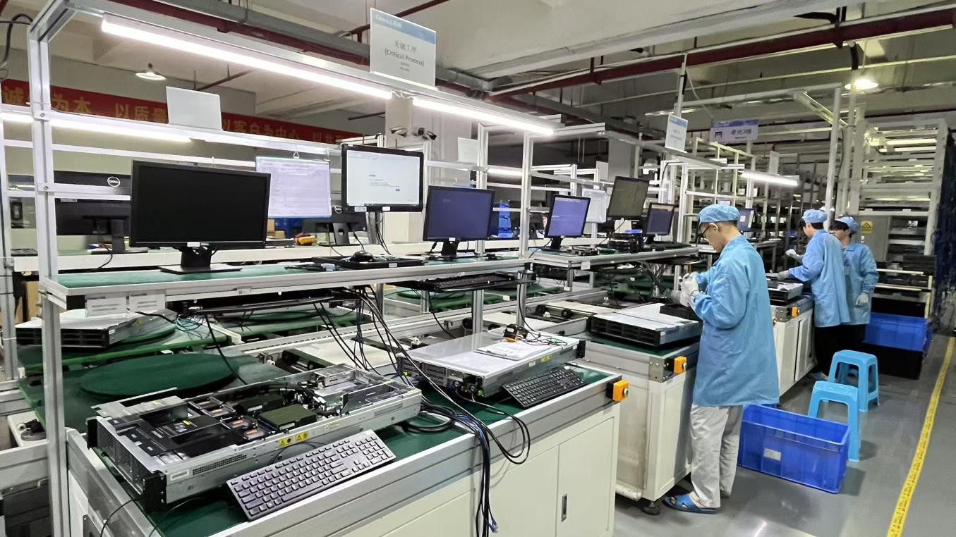

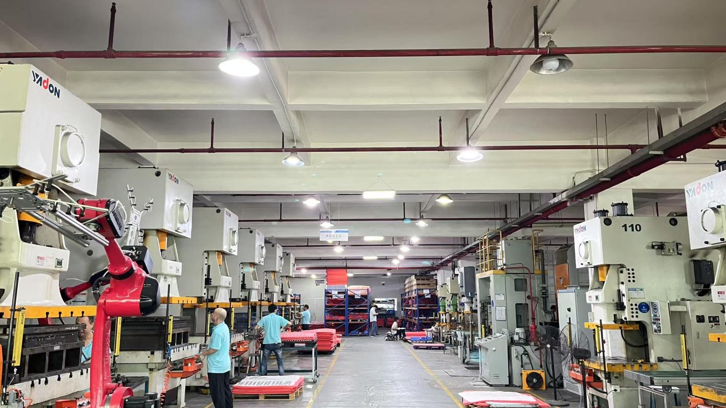
Innovation is the core of our business model. Our dedicated R&D department features 76 experienced engineers who design, test, and release approximately 138 new products annually. We specialize in comprehensive OEM, ODM, private labeling, custom firmware optimization, and bespoke PCB layout adaptations designed to fit seamlessly into specialized server chassis and industrial cabinets.
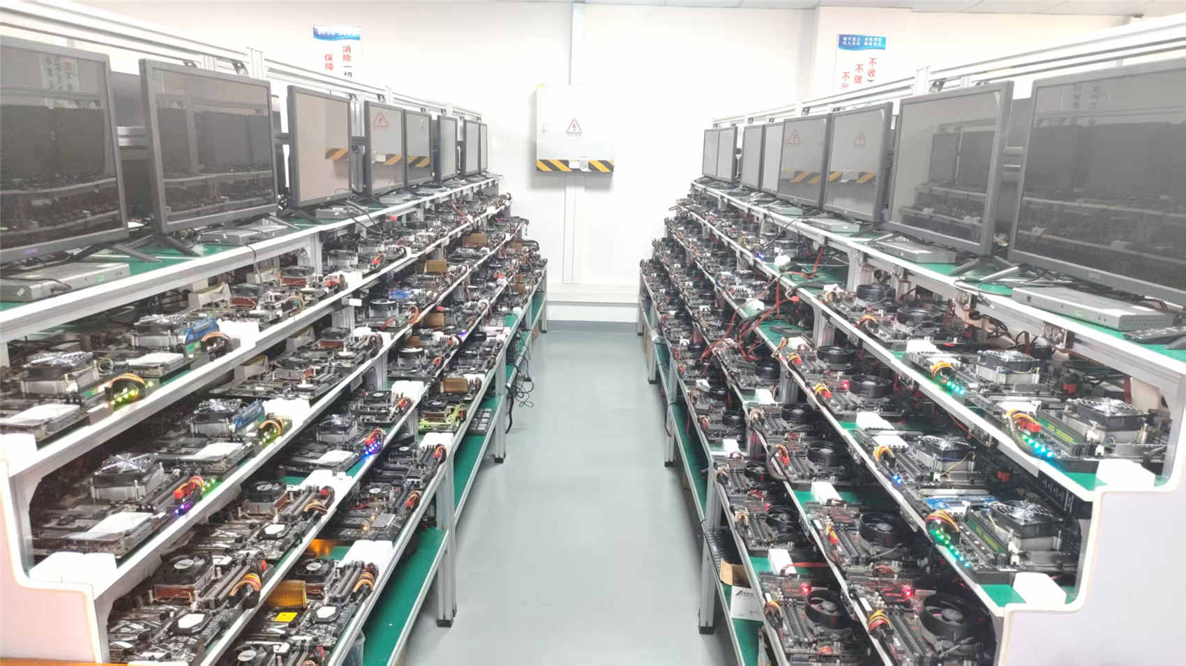
For American electronics buyers, board failures are not just inconvenient—they can lead to costly downtime, product recalls, and liability risks. To prevent these issues, Novram Electronics implements strict testing protocols for every batch of multilayer printed circuit boards and server hardware modules. Our quality control division employs 42 dedicated, professional inspectors who manage quality gates throughout the production cycle.
Before shipping, every assembly undergoes rigorous testing to guarantee reliable field operation, including:
We are committed to environmental responsibility and trade compliance, ensuring all components comply with RoHS Directive (2011/65/EU) and REACH (Registration, Evaluation, Authorization and Restriction of Chemicals) standards. This alignment simplifies import customs processing at US ports of entry.
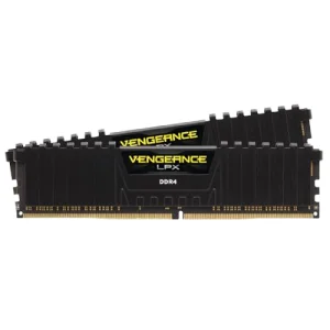
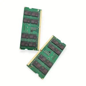
In modern computing architectures, components do not operate in isolation. High-frequency computing systems—such as server blades, processing nodes, and AI network switches—require high-density multilayer PCBs, high-performance DRAM memory modules, and advanced thermal management systems to function reliably. As a single-source engineering partner, Novram Electronics supports this entire ecosystem.
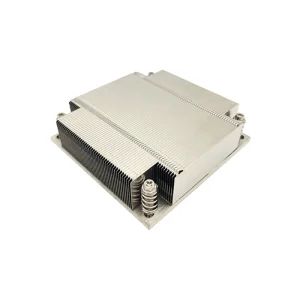
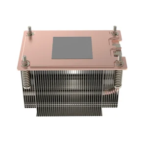
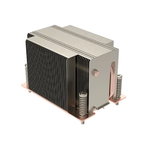
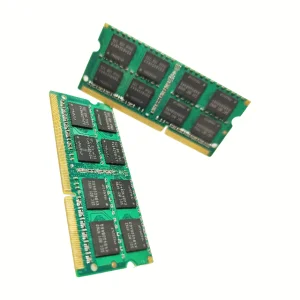
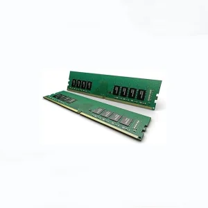
When designing high-layer-count motherboards for servers, signal integrity for memory buses (like DDR4/DDR5) is highly sensitive to layout design. The routing traces require tight impedance controls to prevent signal degradation at gigabit transfer rates. Additionally, high-performance CPUs and memory modules generate significant heat during heavy workloads. Without copper-core vias, passive heat dissipation paths, or custom server heatsinks, thermal build-up can degrade motherboard components and shorten their lifespan.
By offering a unified catalog of high-Tg multilayer PCBs, DDR4/DDR5 memory modules, and specialized aluminum and copper passive coolers, Novram enables U.S. hardware designers to purchase complete, pre-validated subsystem platforms. This integration simplifies system assembly, ensures structural compatibility, and reduces supplier-coordination overhead for procurement teams.
To keep pace with the fast-moving electronics industry, Novram continuously refines our fabrication technologies and product standards. Our research and development focuses on three primary fields:
Developing Semi-Additive Processes (SAP) to enable ultra-fine traces down to 2/2 mil space-width configurations, helping designers shrink system form factors while improving routing density.
Optimizing custom multilayer layout templates to support high-speed DDR5 signaling up to 6400 MT/s, using advanced copper foils to minimize signal attenuation.
Integrating direct-contact 3D vapor chambers with specialized heatsinks, providing efficient thermal management for processors running workloads up to 350W.
Review comprehensive answers to common questions about advanced multilayer PCB manufacturing, material specifications, and global logistics.
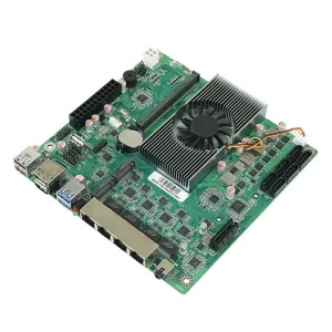
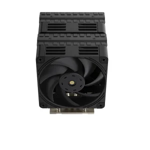
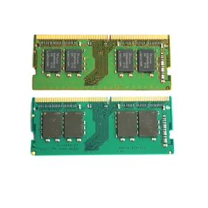
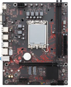
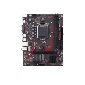
Find the components you need for your system integrations, including server radiators, DDR memory modules, and specialized motherboards.
Get in touch with our engineering team to discuss your multilayer designs, thermal requirements, or custom memory module specifications.