Novram
Novram
Novram
Established in 2016, Novram Electronics Co., Ltd. has developed from a dedicated memory module developer into an integrated manufacturer of advanced multi-layered printed circuit boards and processing systems. Our high-density substrates serve as the structural and electrical backbone for server systems, computing modules, and enterprise electronics globally.
Within high-performance hardware systems, signal speed and thermal dissipation rely directly on substrate integration. At Novram Electronics Co., Ltd., we design and manufacture complex multilayer PCBs (ranging from 4 to 32+ layers) engineered to handle ultra-high frequency signals, minimize impedance variations, and manage dense routing challenges. Our facility in Shenzhen, China, integrates raw substrate production with advanced SMT (Surface Mount Technology) assembly line processing, delivering vertically integrated products that meet strict international specifications.
Through close coordination with 860+ qualified supply chain partners, we secure high-performance copper clad laminates (such as Rogers, Megtron, and Panasonic families) to maintain stable production capabilities. Our manufacturing floor features automated optical inspection (AOI) systems, X-ray laminating registration controls, and flying probe testers, ensuring that every board structure is fully verified before thermal or component integration.
From our 3,860㎡ factory in Shenzhen, we provide end-to-end capabilities spanning layout consultation, substrate fabrication, component mounting, and thermal integration. With 9 years of industry experience and 7 years of export history across 40+ countries, we assist engineering teams in transforming layouts into robust hardware assemblies.
As signals shift from megahertz to high-gigahertz ranges, standard FR-4 materials face physical limitations. Our technological development addresses high-speed routing challenges through specific mechanical advancements.
Modern layouts demand minimized dielectric constant (Dk) and dissipation factor (Df) values. We supply boards built on high-grade materials that limit signal loss and skin-effect resistance at frequencies exceeding 28 GHz, crucial for PCIe Gen 6 and high-speed data networking interfaces.
By replacing conventional mechanical drilling with ultraviolet laser systems, we produce microvias down to 75µm. Any-Layer HDI (Every Layer Interconnect) allows stackups that run vias across all layers, optimizing trace routing and signal path efficiency for mobile and computing modules.
To maximize board space and reduce parasitic inductance, our manufacturing capabilities integrate passive resistors and capacitors directly into inner layer structures. This technology leaves the outer surface free for active IC components and high-pin-count BGA packages.
High-power systems require robust heat dissipation. Our heavy-copper PCB designs utilize inner layers with up to 6oz of copper thickness. Combined with thermal vias and embedded copper coins, these boards conduct heat away from components toward external cooling hardware.
We deliver specialized circuit boards configured for target environments, balancing electrical performance, thermal dissipation, and long-term operating durability.
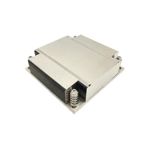
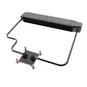
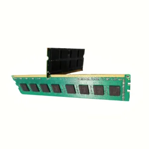
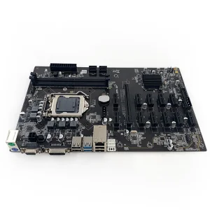
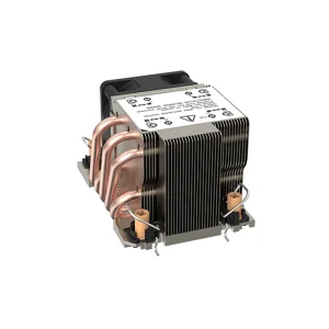
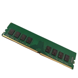
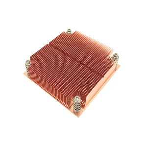
Our server-class PCBs support backplane architectures with up to 32 layers. Engineered with controlled impedance configurations, these boards support high-bandwidth memory modules, PCIe Gen 5/6 routing, and 1U/2U server cooling radiator arrays.
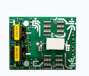
Industrial hardware demands high reliability under thermal stress. We build robust driver boards (like ZX7 series welding machine systems) with thick copper plating, ensuring reliability under consistent thermal cycles and heavy current demands.
By using high-frequency substrates with precise dielectric constants, we manufacture radio frequency and antenna PCBs for high-speed network systems. Our controlled impedance processes help minimize signal distortion across transmission runs.
Located in Shenzhen's electronics ecosystem, our manufacturing facility coordinates raw material sourcing, fabrication, assembly, and testing within a unified system.
Our facility runs automated inline systems linking production steps. By integrating Laser Direct Imaging (LDI) with optical positioning systems, we maintain layout registration accuracy within ±25µm. Our multi-stage vacuum laminator applies heat and pressure curves to help prevent void formation, key to ensuring insulation reliability in high-layer count boards.
Operating in Shenzhen allows us to source copper foils, specialized prepregs, and electronic components directly from 860+ vetted suppliers. This proximity streamlines material procurement, enabling us to manage lead times effectively and scale production to meet project demands.
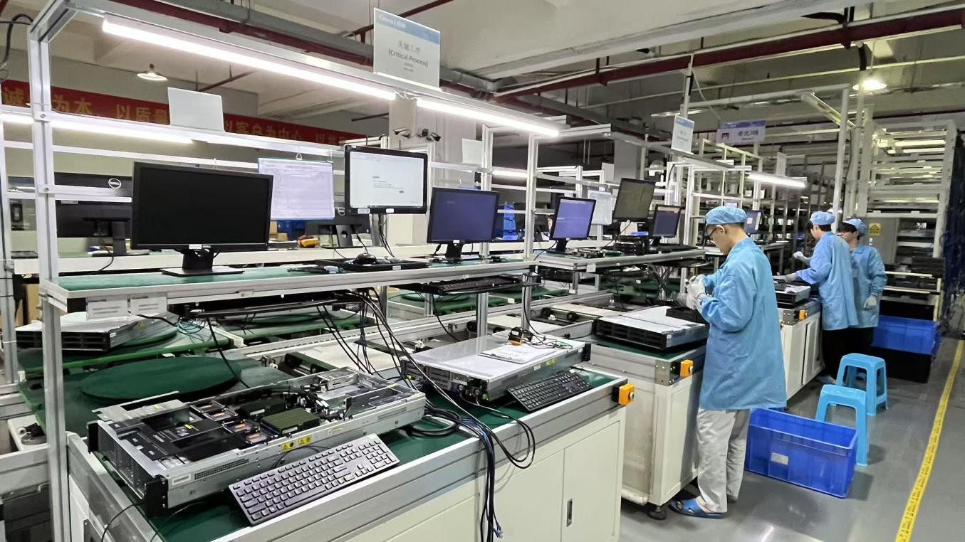
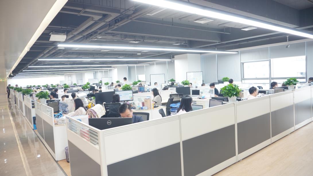
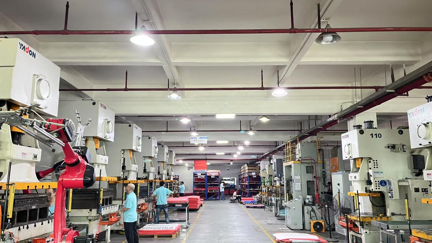
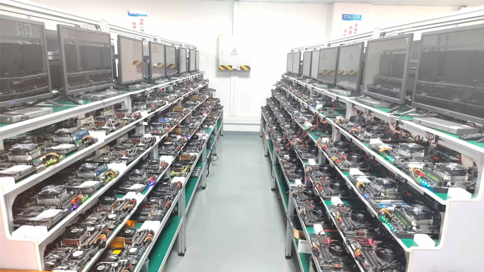
Factory view: Inline cleanroom assembly areas, high-speed automated placement machinery, and multi-layer thermal bonding chambers.
Every PCB and subassembly undergoes structured inspection steps managed by our 42 quality control technicians to verify performance under thermal and electrical stress.
We perform 100% automated optical inspection (AOI) to check for trace defects, plus X-ray transmission checks to verify layer alignment. Cross-sectional microsectioning checks copper thickness plating within vias.
Thermal stress testing subjects boards to float cycles at 288°C, measuring substrate integrity. We also run temperature-humidity bias testing (THB) and high-temperature burn-in tests to identify potential failures.
Time-domain reflectometry (TDR) measurements verify trace impedance parameters within specified limits. All boards and subassemblies comply with UL 94V-0, RoHS, and REACH environmental requirements.
With 76 development engineers producing multiple new designs annually, we collaborate with external teams to refine board layouts, specify stackups, and match production parameters to system needs.
Our engineering division assists customers from prototyping through high-volume production runs. Through Design for Manufacturability (DFM) reviews, we analyze trace routing, via placement, and plane configurations to limit defects during production phases.
We build customized layer stackups for single-ended or differential signals, utilizing Polar Instruments calculation software to define target dielectric heights and trace widths.
We supply boards with flat finishes suitable for fine-pitch component placement, including Electroless Nickel Immersion Gold (ENIG), OSP, Immersion Silver, and Lead-Free HASL.
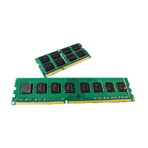
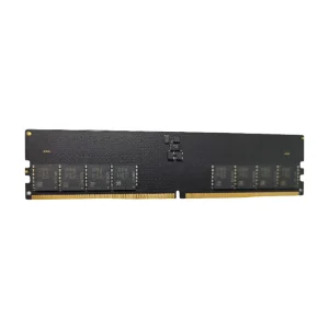
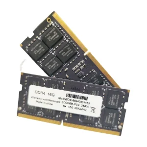
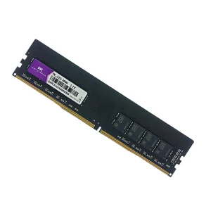
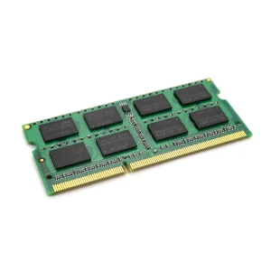
For full system integration (such as memory modules or controller assemblies), we source active components from verified manufacturers and run compatibility testing.
We offer laser marking for unit tracking, custom ESD packaging layout design, and component tracking records for enterprise projects.
Answers to technical and logistical questions for global procurement and engineering teams.