Novram
Novram
Novram
The global transitions toward high-power solid-state lighting, smart city infrastructure, and intensive automotive electrification have forced electronic engineers to re-evaluate the core foundation of thermal management: the Printed Circuit Board (PCB). Modern High-Brightness LEDs (HB-LEDs) dissipate substantial thermal energy within limited spatial profiles. If left unchecked, this thermal burden reduces luminous efficiency, causes color shifting, and ultimately brings premature module failure. Consequently, the sourcing of custom Metal Core Printed Circuit Boards (MCPCBs) and high-density, multi-layer thermal architectures is no longer a simple transactional purchase, but a key structural design choice.
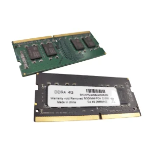
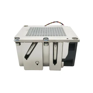
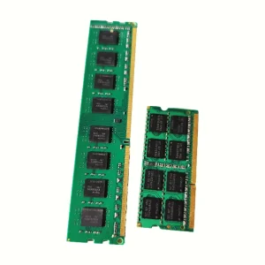
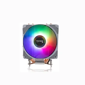
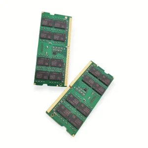
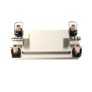
Novram Electronics Co., Ltd., founded in 2016 in Shenzhen, China, stands at the intersection of high-precision electronic layouts and advanced thermal design. Over 9 years of production expertise and 7 years of intensive export operations across 40 countries, we have developed advanced technologies for computing hardware—exemplified by high-speed DRAM modules and multi-heat-pipe server coolers—allowing us to master high-performance metal substrates, resin plug via processes, and extreme-density copper cladding designs. This document details the technical dynamics, manufacturing standards, and structural developments of modern LED circuit boards.
Modern LED circuit boards require advanced substrate materials to ensure heat is transferred away from the junction point of the light-emitting semiconductor. The selection of the base material directly dictates the lifetime and reliability of the end product.
Utilizing aluminum or copper bases bonded to a thin dielectric layer, MCPCBs provide up to 8W/m·K of thermal conductivity, reducing junction temperatures under heavy current loading.
For multi-layer LED driver arrays, we employ TG-170 or TG-180 FR-4 glass epoxy. This ensures structural integrity, low thermal expansion coefficients (CTE), and resistance to thermal stress.
By using 3oz to 6oz copper cladding, we increase the cross-sectional area of traces. This allows high currents to be carried safely while also dispersing heat across the board's surface.
Choosing the correct dialectric layer is critical. Standard FR-4 displays a thermal conductivity of approximately 0.25 W/m·K, which acts as a barrier to heat transfer in high-density LED arrays. By contrast, our custom-engineered insulated metal substrates (IMS) feature micro-thin dielectric layers (from 50μm to 150μm) filled with ceramic polymers. This architecture provides high dielectric breakdown voltage (exceeding 4kV to 6kV AC) alongside excellent heat transfer characteristics. This ensures compliance with international electrical safety standards while protecting sensitive components from thermal degradation.
Technical Insight: To minimize thermal resistance, engineers must pay close attention to the interface between the metal core and the heat sink. Using direct thermal paths—such as thermal vias connected directly to the copper plane—can reduce thermal resistance by up to 60% compared to traditional surface mounting on standard FR-4.
Industrial buyers and system integrators face unique supply chain challenges in today's electronic manufacturing landscape. Procurement requirements have shifted from low-cost sourcing to quality-driven sourcing models that prioritize technical support, supply chain transparency, and international compliance. Major demands include:
Novram Electronics addresses these needs by combining raw board manufacturing with integrated design support. Armed with 9 years of design and manufacturing experience, our team of 76 R&D engineers supports global procurement departments through Design for Manufacturability (DFM) reviews. This process helps resolve issues early, preventing costly assembly reworks and reducing overall time-to-market.
Ensuring the long-term reliability of LED circuit boards operating in demanding industrial environments requires a controlled, multi-stage testing regimen. At Novram, quality control is integrated into every step of the manufacturing process rather than being treated as a final check before packaging.
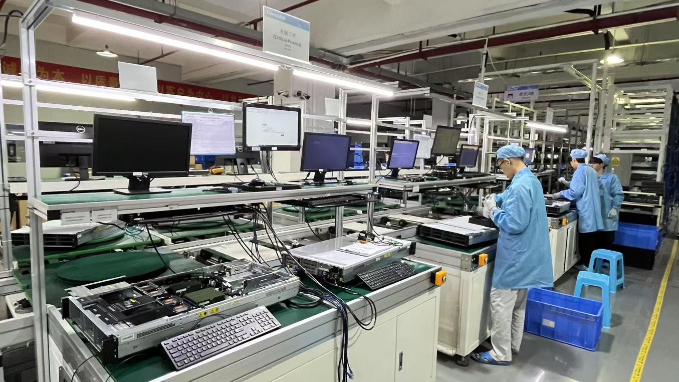
Drawing on our experience in manufacturing high-frequency DDR5 memory modules and high-wattage server cooling systems, we apply rigorous quality assurance methodologies to our LED circuit board lines. The production sequence is governed by 42 dedicated quality inspectors using advanced testing equipment:
Pre-reflow and post-reflow high-speed cameras check trace geometries, paste deposit alignments, and component placement tolerances to prevent dry joints or bridges.
For high-power LED pads, we verify that voiding within the thermal path remains below 10%, ensuring a clear channel for heat dissipation away from the LED chip.
Insulation and dielectric breakdown voltages are tested at high levels to verify that the insulating layer will remain stable under field conditions.
Additionally, all metal-core configurations undergo strict thermal shock and environmental chamber testing. Boards are cycled repeatedly from -40°C to +125°C to detect internal delamination between the metal base, dielectric polymer, and copper foil. By sourcing materials from over 860 approved suppliers, we maintain excellent consistency in raw materials, protecting your production line from variations in substrate performance.
Looking to the future, several technological trends are shaping the development of next-generation LED circuit boards:
Embedded Drivers and Passive Components: To save space, designers are moving away from external driver modules. Multi-layer structures now embed capacitors, resistors, and driver ICs within the internal layers of the substrate. This requires advanced via-in-pad plating, resin plugging, and planar transformer technologies.
COB (Chip-on-Board) and Mini-LED Backlighting: The trend toward ultra-thin displays and architectural lighting has accelerated the adoption of COB and Mini-LED technology. In these setups, bare LED dies are mounted directly onto high-density gold-plated circuit paths. This demands extremely tight routing tolerances and excellent surface planarity, which are achieved through advanced chemical plating techniques (ENEPIG).
Sustainable and Halogen-Free Materials: Environmental regulations are driving demand for halogen-free, bio-degradable, and easily recyclable substrate alternatives. Novram is continuously researching and adopting green manufacturing techniques to align with global environmental requirements.
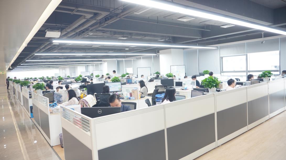
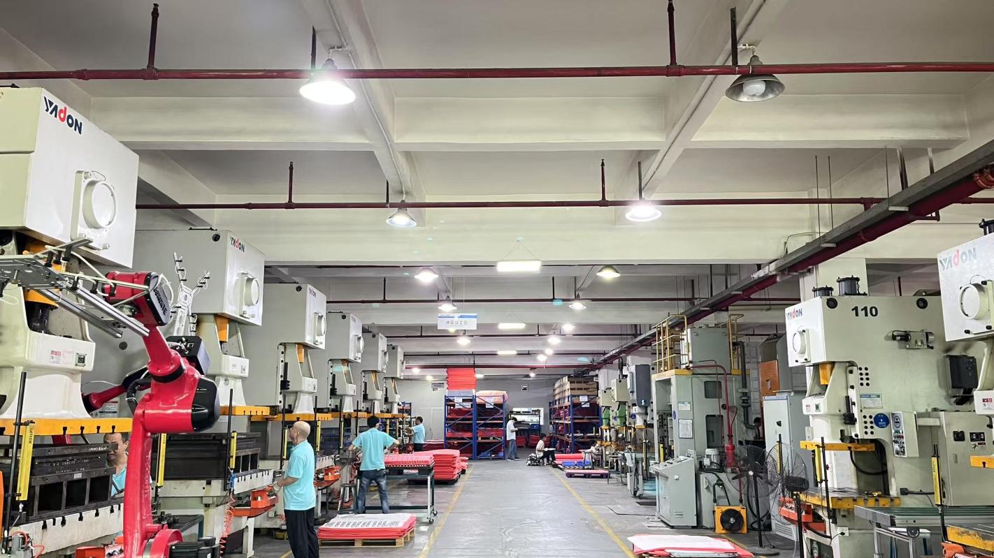
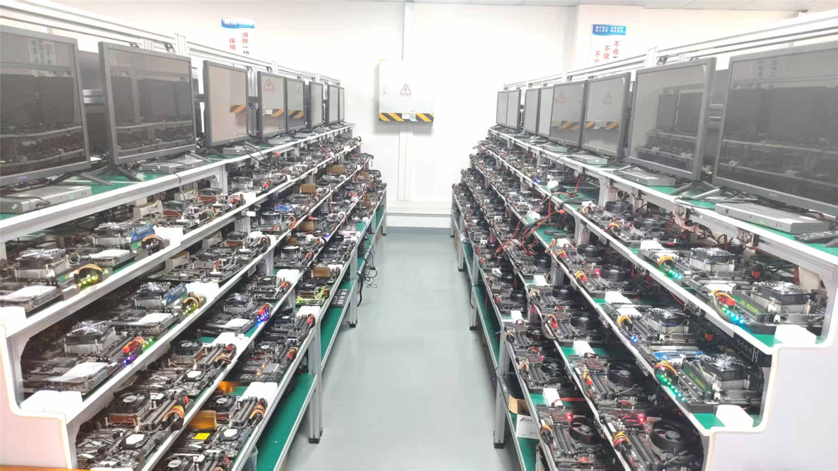
Exporting custom electronic products to a global client base demands more than manufacturing capabilities; it requires strict adherence to international regulatory frameworks. Over our 7 years of active export operations, Novram has built a regulatory and logistical network designed to ensure smooth, compliant deliveries across North America, Europe, Asia-Pacific, and South America.
Our manufacturing facilities are fully compliant with RoHS and REACH regulations, ensuring that all circuit boards, solder mask chemistries, and finishes are lead-free. Furthermore, we maintain UL safety certifications for our substrates, ensuring our products can be easily integrated into end-user equipment seeking local UL, CE, or FCC approvals.
Logistically, we utilize optimized packaging strategies designed to prevent moisture absorption and electrostatic damage (ESD) during long sea or air shipments. Our customer service team coordinates directly with your custom agents, providing complete HS code classifications, certificates of origin, and comprehensive compliance documentation to prevent port clearance delays.