Novram
Novram
Novram
Tailored high-performance hardware and complex circuitry built for direct deployment in Peru’s telecom nodes, high-altitude mines, and heavy industries.


Peru's economy is undergoing a massive structural transformation, driven by large-scale mining operations (especially in regions like Arequipa, Cusco, and Moquegua), rapid expansion of regional telecommunications, and modernization of infrastructure networks. The environmental and geographical settings in Peru present unique, harsh operating environments for complex electronics.
High-altitude deployments (often exceeding 4,000 meters above sea level in the Andes) pose severe physical challenges: lower atmospheric density significantly limits standard convective air cooling, while wide diurnal temperature oscillations strain physical component interfaces through cyclic thermal expansion and contraction. Combined with the high concentration of airborne abrasive particulate matter from open-pit mining operations and high relative humidity near coastal ports like Callao, standard consumer-grade electronics are highly vulnerable to premature field failure.
To operate reliably under these conditions, industrial-grade multi-layer printed circuit boards (PCBs) must incorporate structural safeguards. These include using High-Tg (Glass Transition Temperature) FR-4 base materials to maintain mechanical integrity under thermal stress, thick copper claddings to support heavy electrical loads, and advanced surface finishes such as Electroless Nickel Immersion Gold (ENIG) to prevent atmospheric corrosion. As a reliable manufacturing partner, Novram Electronics designs and manufactures high-density interconnect (HDI) and multi-layer PCBs engineered to meet these environmental challenges.
Specialized PCB stack-ups designed with integrated thick thermal copper cores and heavy-duty sink mounts to handle low-pressure air conditions.
Automated conformal coating applications protecting active signal layers from ambient high humidity and airborne particulate contamination in mining sites.
Strict controlled impedance matching and differential pair routing configurations protecting mission-critical telemetric tracking from electromagnetic noise.
A solid production capacity built to support complex global supply chains and high-volume industrial rollouts.
Our manufacturing processes are engineered to provide maximum precision, signal integrity, and long-term durability under demanding industrial conditions.
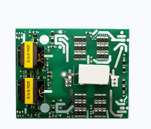
In modern electronic systems, high-density multi-layer printed circuit boards serve as the core platform for system performance. Novram Electronics manufactures multi-layer PCBs ranging from 4 to over 32 layers. These boards are built using advanced processing techniques designed to handle high frequencies and ensure clean signal paths.
Reliable multi-layer performance relies on stable design architecture. Our engineering team designs stack-ups with precise dielectric thickness, controlled trace spacing, and optimized ground plane returns to minimize crosstalk and electromagnetic interference (EMI). We support high-density routing by integrating blind vias, buried vias, and microvias. This allows for clean routing to fine-pitch components (such as 0.4mm pitch BGAs) and improves signal integrity for high-speed applications.
| Feature / Parameter | Standard Capability | Advanced / Custom Capabilities |
|---|---|---|
| Layer Count | 2 - 12 Layers | 14 - 32+ Layers |
| Base Materials | Standard FR-4 (Tg 135-150) | High-Tg FR-4 (Tg 170-180), Rogers, Polyimide, Halogen-Free |
| Finished Copper Thickness | 0.5 oz - 2.0 oz | 3.0 oz - 6.0 oz (Heavy Copper for Power Distribution) |
| Minimum Trace Width / Spacing | 4 mil / 4 mil (0.1mm) | 3 mil / 3 mil (0.075mm) (High Density HDI) |
| Surface Finish Options | HASL Lead-Free, OSP | ENIG (Electroless Nickel Immersion Gold), Hard Gold plating, Immersion Silver |
| Impedance Control Tolerance | ±10% | ±5% (High Frequency & RF Circuits) |
Material quality directly affects how a board performs under continuous heat and mechanical stress. Our raw material stock includes options such as KB6160, Shengyi, Rogers, and Taconic. For mining telemetry equipment exposed to high temperatures, we use High-Tg materials to help prevent trace cracking and vias separation. For RF communication infrastructure in urban centers like Lima, we use low-loss Teflon and Rogers substrates to minimize signal attenuation at higher gigahertz bands.
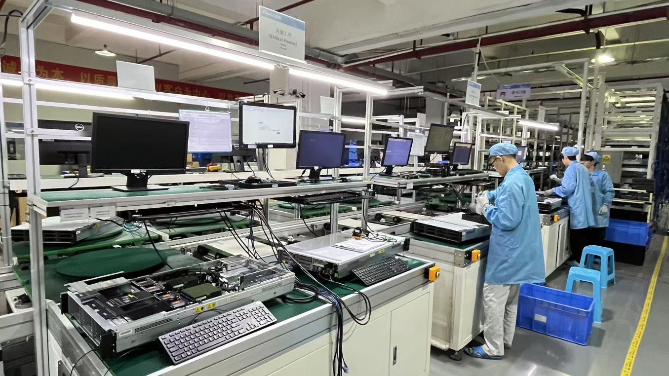
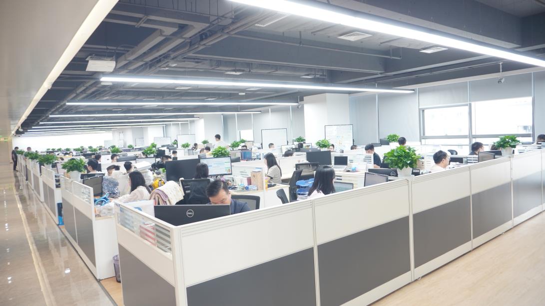
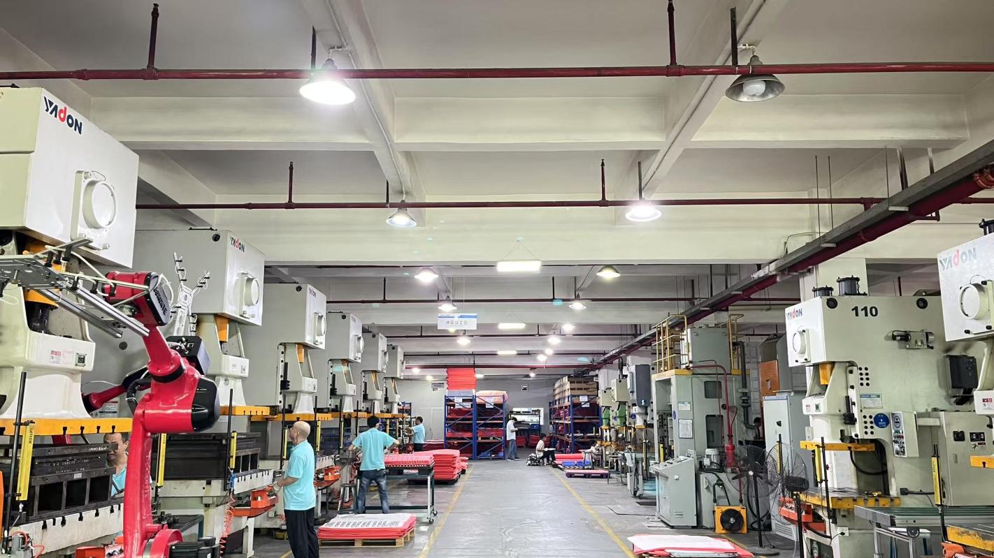
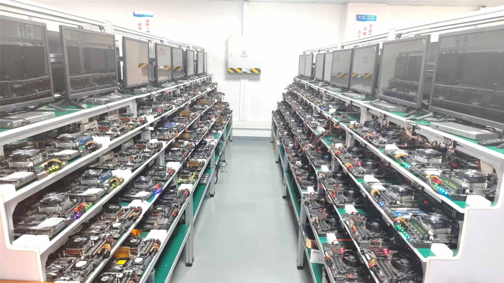
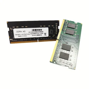
Founded in 2016 in Shenzhen, China, Novram Electronics Co., Ltd. is a specialized electronics and PCB manufacturer. We deliver high-reliability DRAM components and multi-layer printed circuit board solutions for global OEM, ODM, and industrial enterprises. Operating from our modern 3,860㎡ manufacturing facility, we integrate advanced manufacturing technology and strict quality controls.
Over our 9 years of industry experience and 7 years of export experience, we have built a supply footprint covering 40 countries, generating an annual export revenue of approximately US$18.6 million. Our factory is equipped with automated SMT placement lines, high-speed multi-axis drilling machines, and advanced reflow ovens to handle complex double-sided and multi-layer PCB builds.
We work with 860 qualified supply chain partners, enabling us to secure raw materials even during supply shortages. Our client base includes system integrators, telecom equipment suppliers, industrial PC manufacturers, and distributors in Peru and wider South American markets. Our 76 experienced engineers design and release approximately 138 new products each year, supporting a range of customization options from custom board dimensions and layering configurations to specialized firmware optimization.
Our boards are designed for high durability, providing stable performance across mining operations, telecommunications networks, and utility grids.
Our multi-layer boards are built to withstand high vibration, shock, and thermal shifts in heavy mining equipment operating in high-altitude regions like Arequipa and Cusco.
Telecom transmission equipment requires high-frequency substrates and precise controlled impedance. Our designs support stable signal transmission for rural telecommunications setups.
We build heavy-copper PCBs (up to 6oz) to support high current demands and thermal management in grid systems, solar array converters, and inverters.
To ensure high reliability, Novram Electronics implements a multi-step quality control system. Our quality department of 42 professional inspectors tests all boards through a structured verification process:
Shipping custom electronics to Peru requires careful coordination, proper regulatory compliance, and reliable logistics planning. Novram Electronics provides end-to-end support for international shipments, ensuring boards meet local requirements and clear customs smoothly.
We supply complete documentation packages to assist with import clearance at port entries like Callao and Jorge Chávez International Airport. This includes certificates of origin, detailed HS code classification, and safety datasheets. Our manufacturing meets global industry standards, including UL safety certifications, CE directives, and RoHS environmental guidelines, which simplifies compliance for local installations.
To reduce shipping times, we offer flexible shipping arrangements through logistics partners such as DHL, FedEx, and air/ocean freight brokers. We also provide secure, moisture-proof packaging—including vacuum sealing, anti-static bags, and desiccant packs—to protect electronic assemblies during transit across different climates.
Common technical inquiries regarding material specs, shipping processes, and manufacturing services for the Peru market.
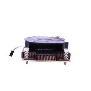
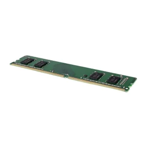
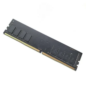
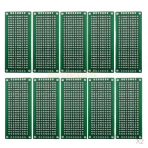
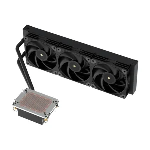
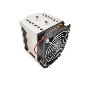
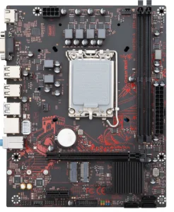
High-performance computational modules, heat management components, and prototyping equipment designed for industrial applications.