Novram
Novram
Novram
The global disinfection landscape is undergoing a monumental transition. Traditional mercury-vapor lamps, which have dominated germicidal irradiation for decades, are being rapidly phased out due to the environmental mandates of the Minamata Convention on Mercury. In this regulatory wake, Deep-Ultraviolet Light Emitting Diodes (UVC LEDs) operating within the 260nm to 280nm spectrum have emerged as the premier ecological and technical alternative.
Unlike legacy gas-discharge systems, UVC LEDs offer instant-on operation, compact form factors, architectural design flexibility, and a lack of hazardous materials. Globally, the industrial demand has shifted from simple surface sanitizers to highly complex, integrated systems: continuous inline water purification, dynamic HVAC airborne pathogen destruction, and high-intensity clinical surface sterilization.
"The critical bottleneck in high-power industrial UVC LED systems is not merely the emission of photons, but the management of thermal energy. Because UVC LEDs currently operate at a Wall Plug Efficiency (WPE) of 2% to 8%, up to 98% of electrical input is converted into destructive junction heat. Advanced thermal substrates and precise electronic drive control are paramount to prevent immediate chip degradation."
As a leading OEM/ODM powerhouse, Novram Electronics Co., Ltd. has leveraged its deep heritage in high-speed semiconductor substrate layout, SMT precision, and industrial heat-sink packaging to pioneer advanced cooling and drive systems specifically optimized for high-flux UVC LED matrices.
The fundamental materials science of UVC LEDs relies on AlGaN (Aluminum Gallium Nitride) epitaxial layers grown on sapphire or silicon carbide substrates. Adjusting the ratio of aluminum determines the exact peak emission wavelength. While 265nm is highly effective for DNA/RNA absorption peaks in standard bacteria, 222nm (Far-UVC) is emerging as a human-safe alternative for occupied spaces, and 275nm remains the sweet spot for commercial longevity and cost-efficiency.
Overcoming dislocations in the crystal lattice of AlGaN is the primary goal of modern UVC LED foundries. High defect densities act as non-radiative recombination centers, dragging down external quantum efficiency (EQE). By utilizing specialized buffer layer techniques and nano-patterned sapphire substrates (NPSS), modern manufacturers have significantly enhanced light extraction efficiency.
| Wavelength Range | Primary Target Applications | Key Material Formulation | Critical Engineering Challenge |
|---|---|---|---|
| 222 nm (Far-UVC) | Occupied public spaces, airborne disinfection, safe skin exposure | High-Al Content AlGaN / KrCl Excimer | Low optical output power & complex band-alignment filtration |
| 265 - 270 nm | Direct biological DNA/RNA disruption, laboratory assay sterilization | Mid-Al Content AlGaN Epitaxy | Maximizing external quantum efficiency (EQE) & light extraction |
| 275 - 285 nm | Municipal water, domestic consumer appliances, surface scanning | Standard AlGaN on Sapphire | Long-term package degradation under extreme UV radiation exposure |
Novram’s product engineering addresses critical integration issues across multiple industrial verticals:
High-flow liquid disinfection requires hermetically sealed quartz-glass barriers and advanced thermal dissipation. Novram’s custom driver boards regulate constant current output to the LED arrays, ensuring consistent irradiance regardless of water temperature fluctuations.
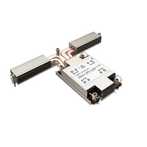
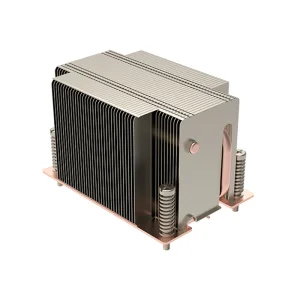
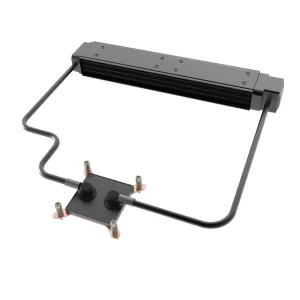
Integrated inside building-wide HVAC ducts, high-power UVC matrices run continuously. Our industrial extruded aluminum radiators and server-grade liquid cooling systems prevent thermal runaway, maintaining LED junction temperatures below 60°C to guarantee a 20,000+ hour operating life.
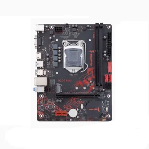
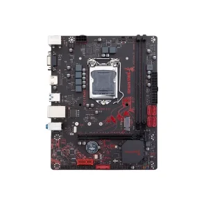
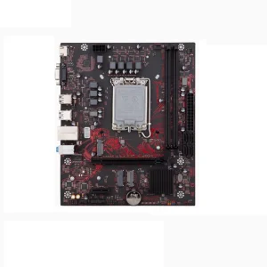
From medical robotics to packaging assembly lines, surface scanners need programmable logic controllers. Our highly-durable motherboards and customized processing kits process real-time sensor feedback to dynamically adjust irradiation intensity based on proximity.
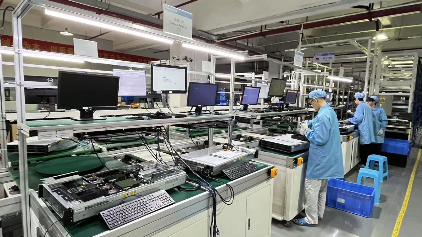
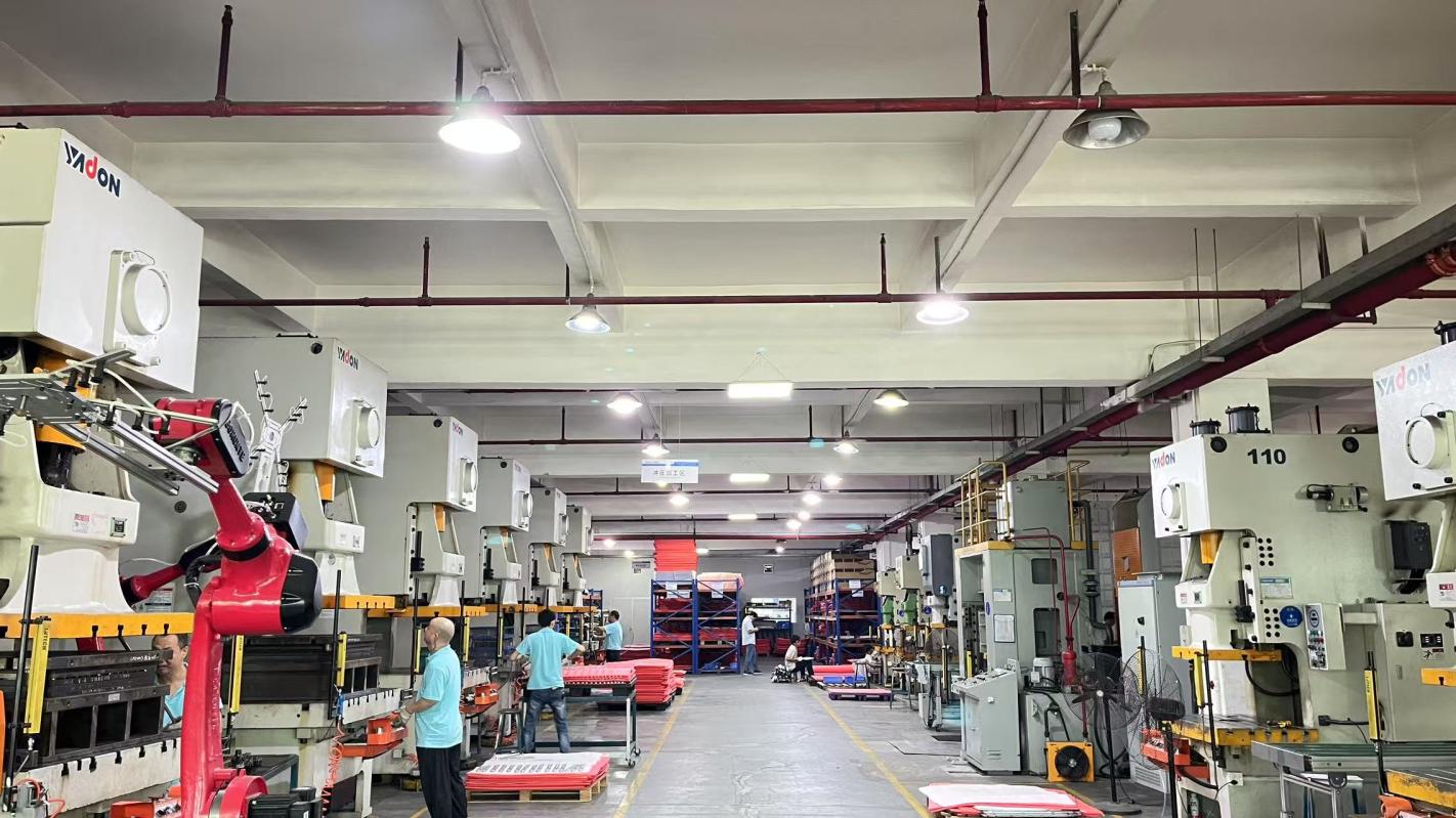
Established in 2016 in Shenzhen, China, the global heart of optoelectronic innovation, Novram Electronics Co., Ltd. has spent nearly a decade perfecting high-density SMT assembly, multi-layer substrate design, and advanced thermal management kits. Operating out of a state-of-the-art 3,860㎡ manufacturing facility, Novram’s factory floor features fully automated Pick-and-Place lines, nitrogen reflow ovens, and cleanroom packaging environments essential for handling sensitive deep-UV components.
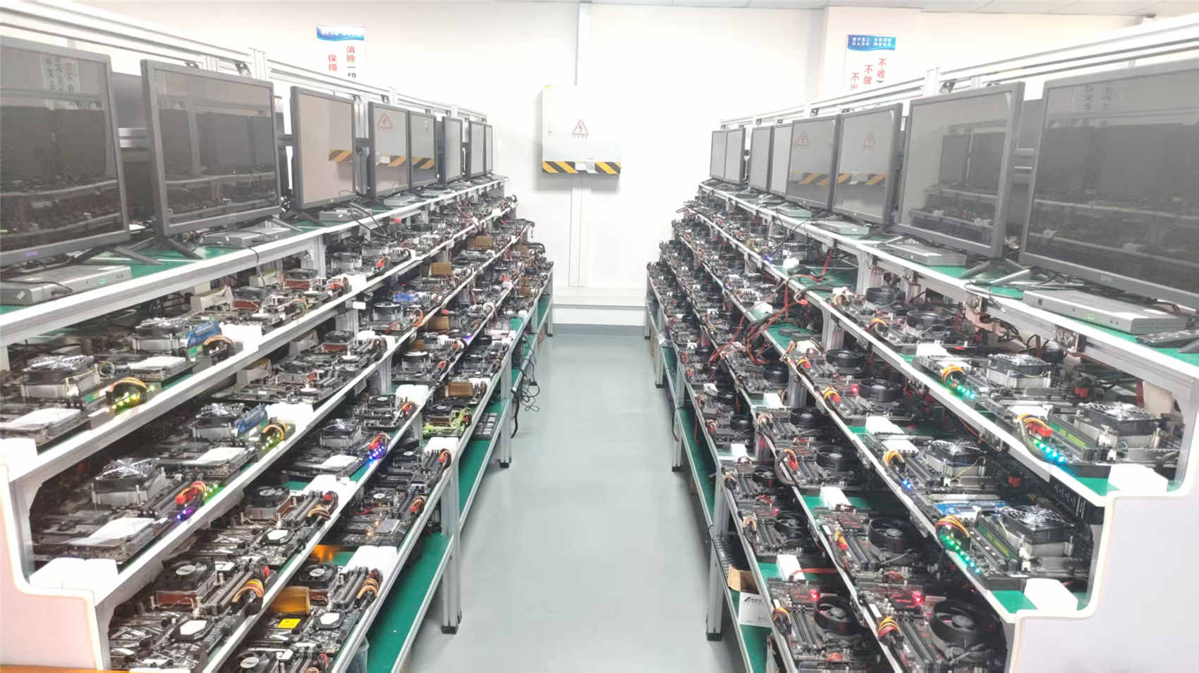
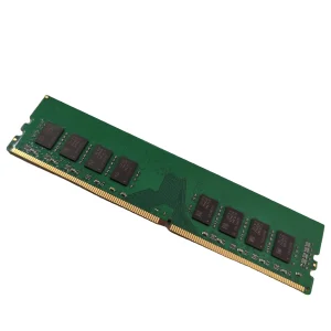
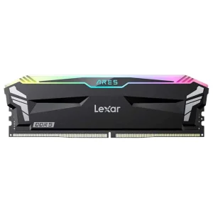
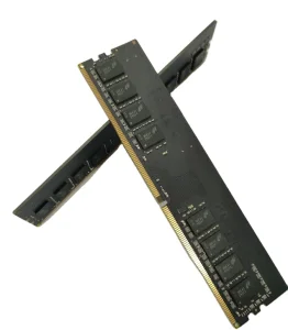
Our core capability lies in bridging the gap between high-precision PCBA (such as high-speed DDR5 DRAM matrices and multi-layered processing motherboards) and high-power optoelectronic system requirements. With over 860 qualified supply chain partners, we source premium materials and electronic components to ensure continuous production reliability. Before any product leaves our floor, it undergoes a rigid multi-stage inspection process conducted by our 42 professional quality assurance inspectors. This includes 100% functional testing, thermal camera burn-in testing, and accelerated aging verification.
Led by a robust team of 76 experienced R&D engineers, we develop custom solutions, releasing up to 138 new specialized products annually. Whether you require tailored private labeling, custom heat-sink geometries for specialized UVC modules, custom driver circuitry, or comprehensive system-level firmware integration, Novram provides full-spectrum OEM/ODM services to memory module brands, industrial PC companies, system integrators, and wholesalers worldwide.
Technical insights and integration guidelines for engineers, system integrators, and procurement directors.
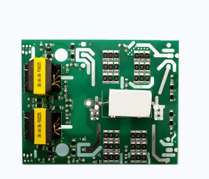
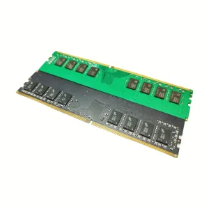
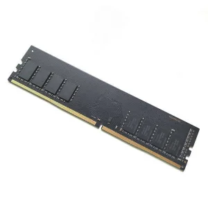
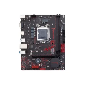
Inside Novram's 3,860㎡ ISO-certified manufacturing facility and quality testing laboratories.