Novram
Novram
Novram
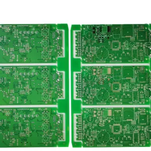
Premium double-sided boards, high-frequency Rogers substrates, server memory units, and custom PCBA prototypes built to global aerospace, industrial, and consumer standards.

In the rapidly advancing era of IoT, 5G communications, artificial intelligence, automotive digitization, and high-performance computing (HPC), Printed Circuit Board (PCB) prototyping has transitioned from a basic testing step to a pivotal milestone in the product research and development cycle. Modern electronics engineering demands rapid-turn prototypes that do not compromise on tolerances, substrate diversity, or mechanical integrity.
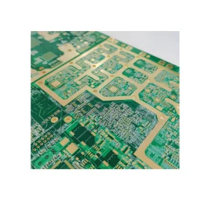
The global PCB prototyping market is witnessing a major transformation driven by three core forces: the miniaturization of electronic devices, the demand for high-speed signal integrity, and the convergence of flexible circuits (Flex and Rigid-Flex PCBs). Advanced multilayer stack-ups utilizing substrates like Shengyi FR4 High TG170 and Rogers 4000 Mixed Pressure have become essential for preventing signal attenuation and structural delamination in high-thermal environments. Prototyping acts as the bridge between theoretical schematic design and volume manufacturing, validating physical layout rules, thermal dispersion efficiency, and component footprint accuracy.
Support for blind and buried microvias, laser drilling, and fine line/space configurations down to 2mil/2mil, critical for dense BGAs in computing units.
Hybrid stackups blending traditional FR-4 with PTFE-based materials (e.g., Rogers 4000 series) to minimize insertion loss and return loss at microwave frequencies.
State-of-the-art Time Domain Reflectometry (TDR) measurements verifying 50Ω single-ended and 100Ω differential trace designs within ±5% tolerances.
Selecting an ideal PCB prototyping vendor and exporter is a strategic decision that heavily impacts engineering velocity and downstream production yield. A failure in the prototyping stage can result in missed market windows, failed compliance testing, or catastrophic thermal failures. Top tier providers are evaluated against strict design-for-manufacturing (DFM) capabilities, lead times, materials access, and testing methodologies.
Understanding where PCB fabrication is heading: AI-driven design rules, advanced material science, and additive 3D-printed circuits.
Additive 3D circuit deposition allows for trace direct-printing on complex curved structures, eliminating traditional wet-chemical etching processes.
Driven by smart wearables and medical implants, multi-layer rigid-flex materials are being compressed below 0.4mm stack thicknesses with ultra-dense signal routing.
Embedding passive resistors, capacitors, and active microcontrollers directly within inner PCB layers to maximize board-surface real estate.
The push for fully biodegradable matrices and halogen-free compounds, minimizing the environmental e-waste footprint of rapid R&D cycles.
Advanced prototyping runs are deeply tailored to the targeted end-use vertical. The performance needs of an industrial automation board operating in high-moisture assembly floors are vastly different from high-frequency server RAM modules processing gigabytes of throughput per second. Here are the core industries deploying our customized PCB designs:
Deploying heavy-copper, multi-layer layouts that handle high-voltage relays, SMT PCBA DIP plug-ins, and high-tolerance connectors. Commonly integrated with immersion silver surface finishes to combat oxidation in harsh factory environments.
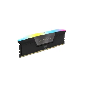
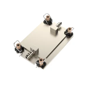
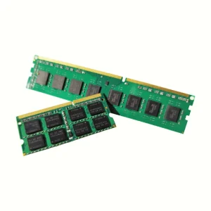
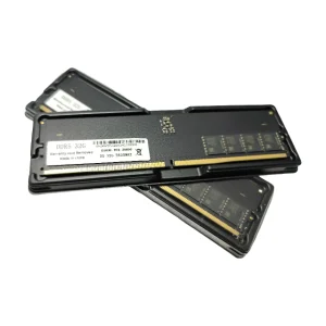
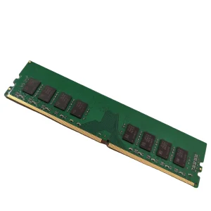
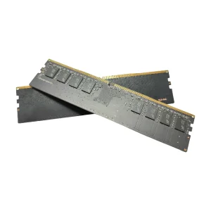
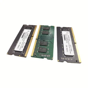
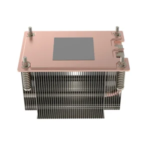
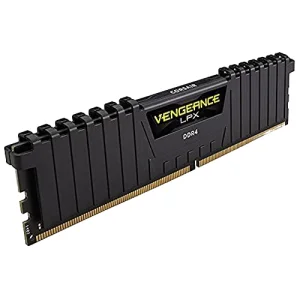
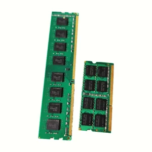
Utilizing high-integrity signal routing for DDR4/DDR5 computer server memory strips, multi-phase power modules, and specialized copper CPU heat sink integrations (e.g., LGA4189 and AM5 200W VC passive coolers) to optimize thermal load distribution.
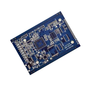
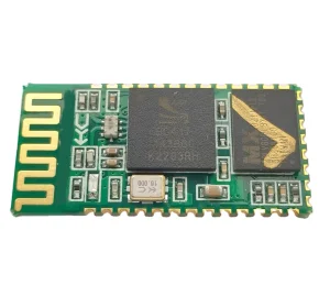
Universal breadboards, multi-layer HDI circuits, and high-sensitivity electronic arrays optimized for specialized applications (such as advanced metal detector coils or handheld sensor instruments).
Discover how a modern Shenzhen-based hardware manufacturer delivers high-performance DRAM solutions and coordinates elite SMT & PCBA prototyping networks globally.
Based in the technology capital of Shenzhen, China, Novram Electronics Co., Ltd. was established in 2016. Over the course of 9 years of industry experience and 7 years of export experience, the company has positioned itself as an industry leader in manufacturing high-performance DDR5 memory modules and facilitating specialized electronics assembly solutions for OEM/ODM, embedded computing, and system integration companies worldwide.
With an annual export revenue of approximately US$18.6 million, Novram supports clients in over 40 countries. Our operations are anchored in strict quality management. Every output component undergoes a comprehensive testing procedure consisting of: 100% functional testing, motherboard compatibility testing, high-temperature burn-in testing, static aging verification, and signal integrity testing. This guarantees that our advanced memory products integrate seamlessly with customized high-frequency boards, power supplies, and industrial PCs.
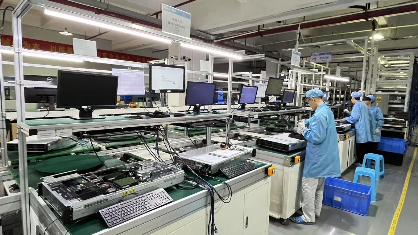
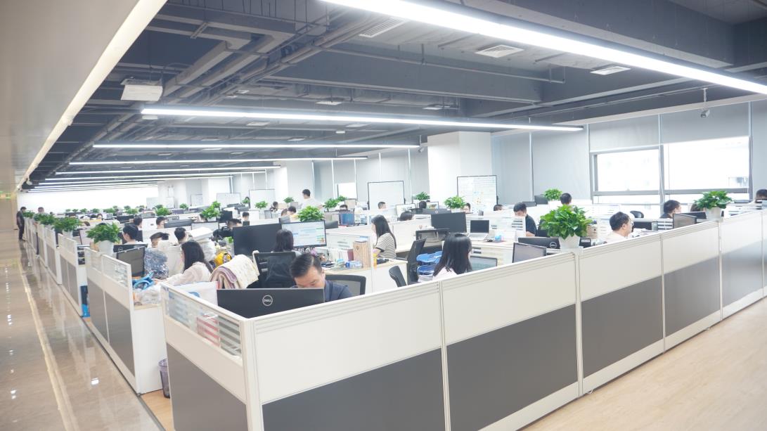
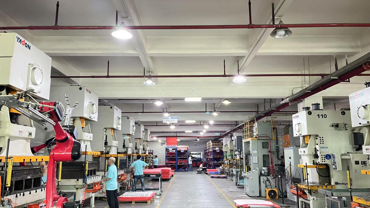
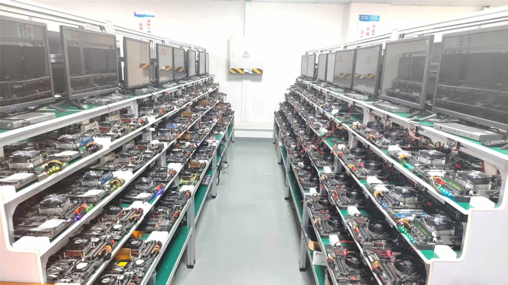
Shenzhen, China represents the world’s most dense cluster for electronics prototyping, substrate fabrication, and components sourcing. This localized ecosystem offers distinct competitive advantages for international hardware engineers looking for PCB prototyping:
In Shenzhen, substrate manufacturers, solder paste vendors, SMT component distributors, stencil laser-cutting services, and advanced logistics providers are located within a 1-hour transport radius. This density enables rapid component sourcing and prompt design iterations, compressing typical 3-week global cycles into less than 48 hours.
Through partnerships with domestic material giants like Shengyi Technology, Chinese fabricators ensure continuous access to high-TG laminates, halogen-free materials, and customized copper foils even during global material crunches. When high-frequency Rogers substrates face long lead times, our engineering network can recommend verified, high-performance domestic equivalents to keep prototyping lines active.
With automated pick-and-place lines running 24/7 alongside skilled DIP plug-in technicians, projects transition from naked boards to functional PCBA prototypes in record time. Advanced testing instruments (AOI, 3D X-ray, flying probe) are standardized across the manufacturing lines to identify soldering defects immediately, ensuring zero-defect dispatches to global exporters.
Exporting high-precision PCBs and RAM modules globally requires strict alignment with localized compliance frameworks, import customs standards, and environmental directives. Partnering with Novram Electronics ensures a secure path for products entering target markets:
All prototypes and assemblies comply with RoHS and REACH regulations. Lead-free surface treatments (like lead-free HASL and ENIG) ensure compliant entry into European and North American markets.
Prototyping boards follow IPC-A-600 (Acceptability of Printed Boards) and IPC-A-610 (Acceptability of Electronic Assemblies) Class 2 or Class 3 parameters, depending on medical/aerospace application requirements.
Anti-static packaging, moisture-barrier bags, and custom commercial documentation prevent clearance issues or transit damage. We offer comprehensive support for global air freight routes.
Frequently asked questions regarding high-frequency substrates, signal impedance, custom SMT assembly, and global delivery logistics.
Explore our collection of reliable server RAM, computer memory modules, performance coolers, and high-sensitivity electronic circuits.