Novram
Novram
Novram
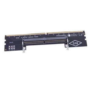
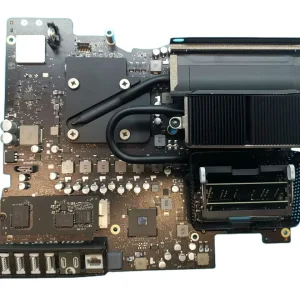
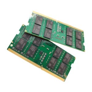
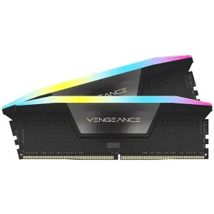
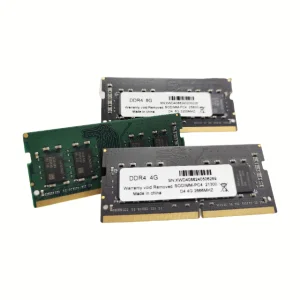
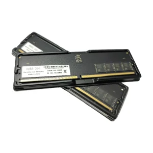
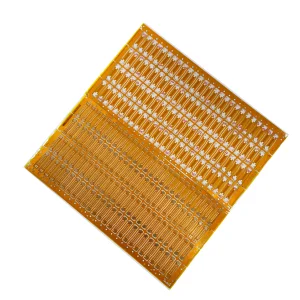
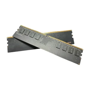
High-yield SMT stencil deposition relies directly on the structural layout of your active PCBs. Below are four key advanced memory and logic boards optimized for Tokyo's robotics, automated assembly lines, and industrial computing infrastructures.
As the epicenter of global robotics engineering, high-end consumer hardware, and automotive microelectronics, Tokyo demands zero-defect execution in surface-mount technology (SMT). From Ota City's precision machine shops to large enterprise electronics facilities in the western Tokyo metropolis, engineers are shifting away from traditional etched stencils to ultra-precise laser-cut solder paste stencils. This evolutionary transition ensures that miniaturized packaging—such as 01005 passives, micro-BGAs, and fine-pitch QFNs—receives the exact volumetric paste deposit required to avoid bridging or voiding defects.
Novram Electronics supports Tokyo's sophisticated SMT lines with high-performance manufacturing. While our high-density DRAM and PCB lines handle complex signal layers, our advanced manufacturing ecosystem coordinates the custom engineering of laser-cut stencils that match Tokyo's tightest pitch tolerances. The local market prioritizes structural durability, strict adherence to aperture aspects, and rapid prototyping capabilities. The integration of high-grade Japanese stainless steel foils with high-speed fiber-laser manufacturing has set new efficiency records across local production plants.
Precision apertures targeting components down to 0.3mm pitches, eliminating bridging and dry-joints in complex assemblies.
Hydrophobic and oleophobic layers that prevent paste sticking, reducing stencil cleaning frequency on the line by up to 60%.
Precisely milled step-up and step-down stencils allowing the co-existence of micro-BGAs and heavy-duty connectors on a single board.
Engineering laser stencils requires adhering strictly to the IPC-7525 guidelines. The volumetric control of solder paste is governed by two physical metrics: the Aspect Ratio and the Area Ratio. In Tokyo's aerospace sensor designs and dense memory PCB modules, maintaining a target Area Ratio greater than 0.66 is critical for excellent paste release.
Our stencils are laser-machined using fiber lasers with a spot size of under 20μm, ensuring clean vertical walls with a slight natural taper that aids paste release. Mechanical polishing or electro-polishing is applied to clear out the microscopic dross and micro-burrs resulting from the thermal laser cutting process. Below are the key manufacturing parameters we monitor:
For high-yield SMT lines in Tokyo, stencil tension and frame design play a vital role. We construct both frameless stencils (compatible with rapid-change foil tensioning systems like ZelFlex or VectorGuard) and permanently mounted aluminum framed stencils. Our dynamic alignment markers (fiducials) are laser-etched half-depth or through-hole filled with black epoxy, ensuring high contrast for automatic recognition cameras on SMT printers like DEK, MPM, or Yamaha machines.
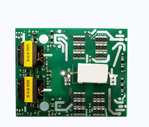
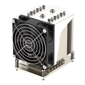
Precision stencil design relies on robust board assembly equipment and mechanical sub-components. These products represent critical hardware supporting SMT printing, drive electronics, and structural cooling interfaces across our manufacturing operations.
In global electronics production, time-to-market determines success. The logistics pipeline between Shenzhen and Tokyo has evolved to offer next-day engineering verification and rapid dispatch. When Tokyo design offices finish their PCB layouts, the Gerber or ODB++ data is uploaded to our engineering portal. Our DFM (Design for Manufacturability) engineers immediately evaluate aperture aspects, component layout pads, and potential solder-balling risks.
Using high-speed laser engraving and automated electro-polishing lines, we produce custom-made laser stencils and ship them directly via premium express services (reaching Haneda or Narita airports within 36 hours). For industrial customers, this provides a highly competitive structure: China's vast material supply chain combined with Japanese-caliber quality assurance. Our manufacturing processes conform strictly to JIS Z 3284 (Solder paste printability standards) and ensure RoHS 3 / REACH compliance on all steel foils, frame adhesives, and chemical nano-coatings.
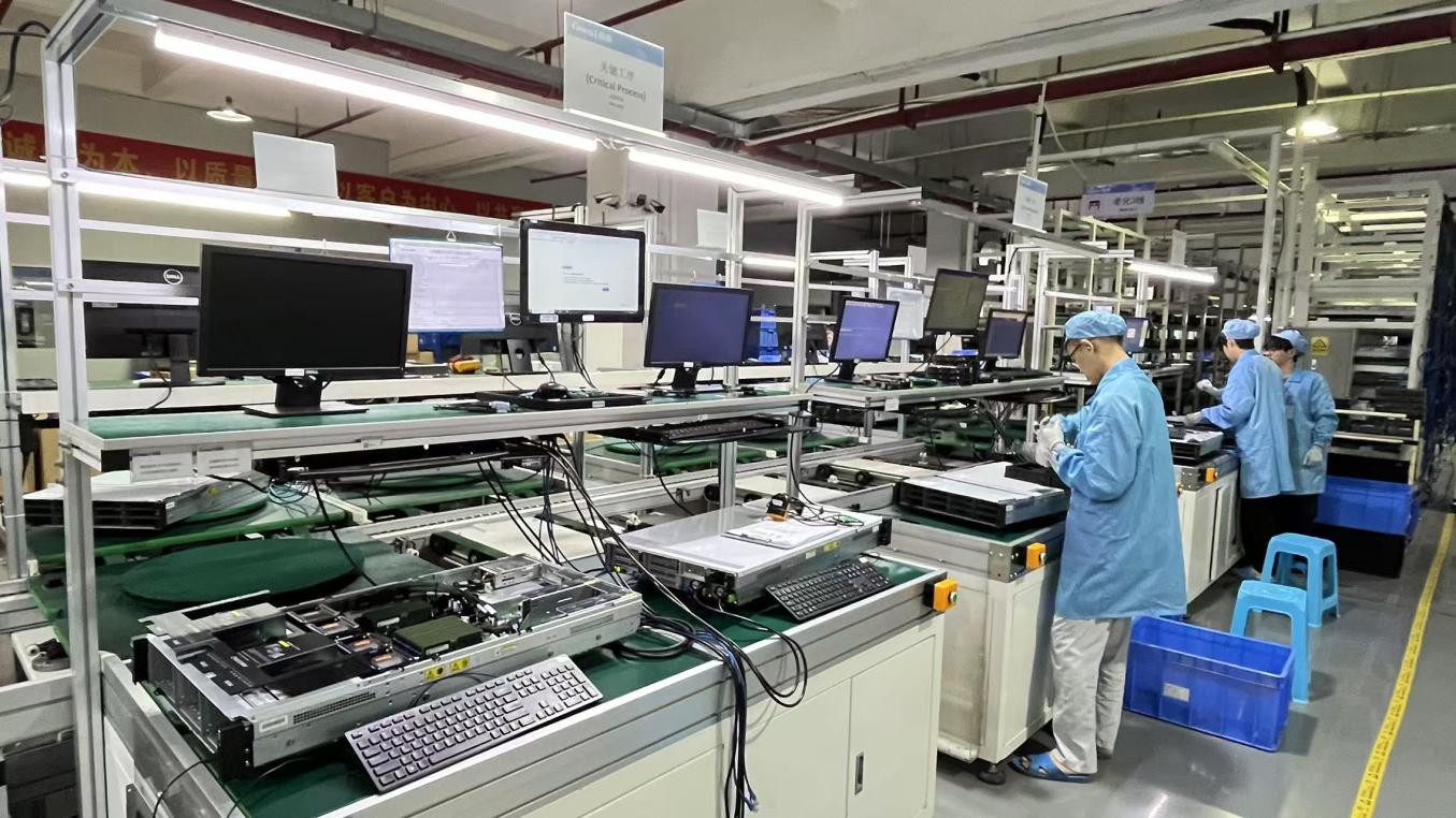
Novram Electronics Co., Ltd. is a professional DDR5 memory manufacturer based in Shenzhen, China, dedicated to delivering high-performance DRAM solutions for global OEM, ODM, and industrial customers. Established in 2016, the company has grown into a reliable supplier of DDR5 memory modules, serving partners across consumer electronics, industrial automation, embedded systems, gaming, and enterprise computing.
Operating from a modern 3,860㎡ manufacturing facility, Novram integrates advanced production equipment, strict quality management, and continuous R&D innovation to ensure every memory module meets international performance and reliability standards. Our experienced engineering team focuses on developing high-speed, stable, and energy-efficient DDR5 products for diverse computing applications.
With 9 years of industry experience and 7 years of export experience, Novram exports products to customers in more than 40 countries. The company achieves an annual export revenue of approximately US$18.6 million, supported by an efficient global supply chain and responsive customer service.
Quality is at the core of everything we do. Every DDR5 memory module undergoes 100% functional testing, compatibility testing, burn-in testing, temperature testing, and aging verification before shipment. Our quality control department consists of 42 professional inspectors, ensuring consistent product performance and long-term reliability.
Novram maintains strong partnerships with over 860 qualified supply chain partners, enabling stable production capacity and reliable component sourcing. Our primary customers include memory module brands, computer manufacturers, industrial PC companies, system integrators, distributors, wholesalers, and OEM/ODM partners worldwide.
Innovation drives our competitiveness. Our dedicated R&D center is staffed by 76 experienced engineers, allowing us to introduce approximately 138 new products each year. We provide comprehensive OEM, ODM, private label, logo printing, packaging customization, capacity customization, firmware optimization, and product specification customization to meet different market requirements.
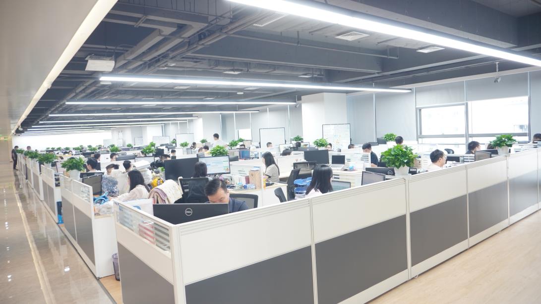
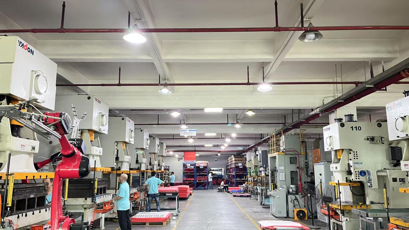
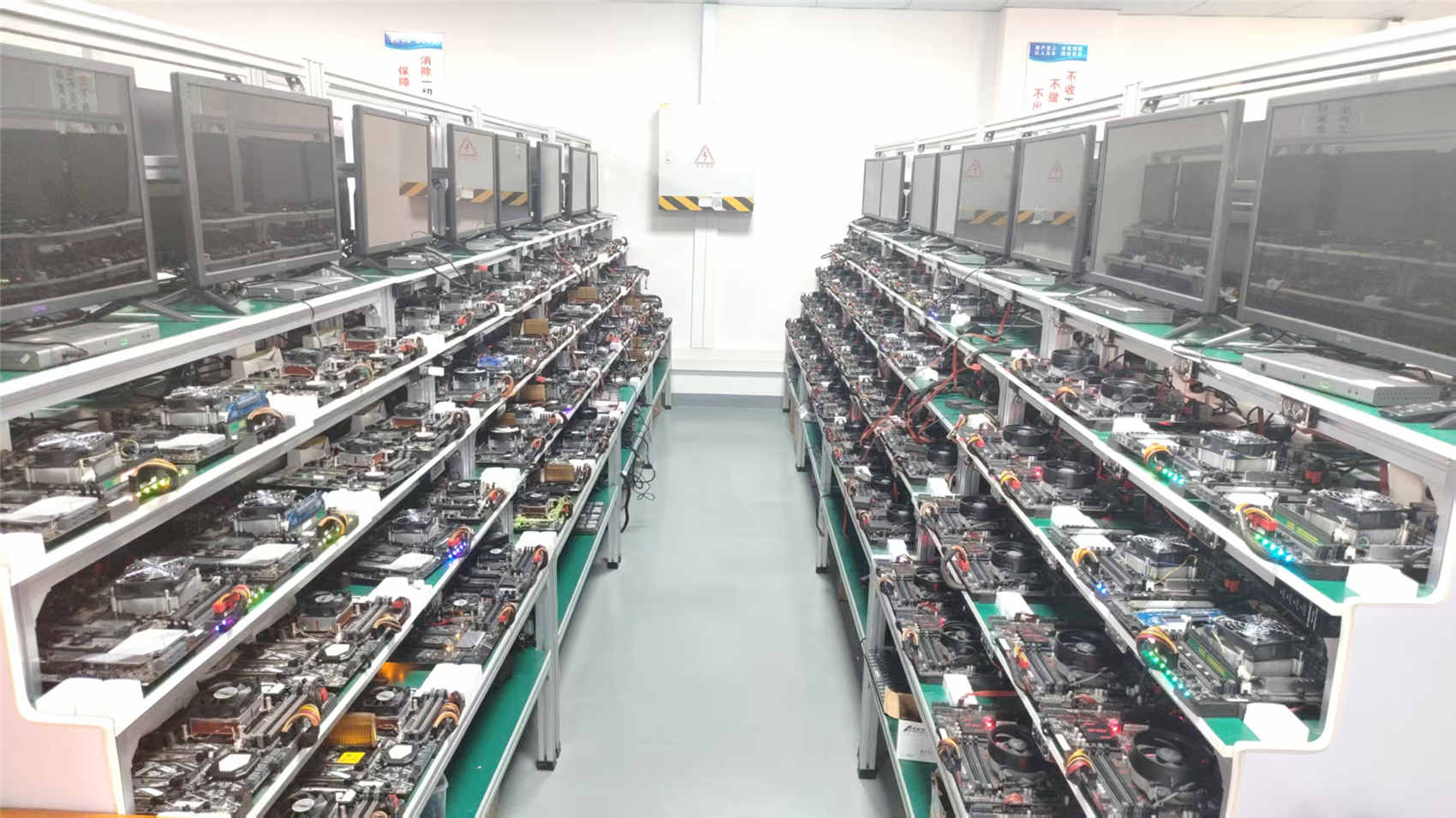
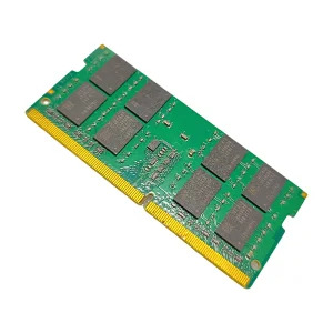
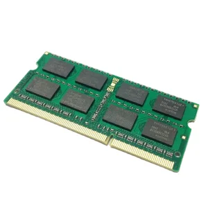
High-density components require optimized solder paste printing. These products, ranging from server RAM to custom flexible PCBs, represent the typical profiles for which our laser stencils are designed and manufactured.
We compile critical inquiries from Tokyo's SMT procurement managers and design engineers to optimize production yields.
Our laser cut systems achieve a position tolerance within ±2μm and size tolerance within ±3μm. This dimensional consistency ensures repeatability during fine-pitch printing operations on high-density PCBs.
Electro-polishing (EP) is highly recommended for components with pitches smaller than 0.5mm, such as BGAs or 0201 passives. EP rounds off micro-dross and reduces aperture wall roughness (Ra) to under 1μm, increasing paste transfer efficiency by up to 25% compared to standard lasers.
All materials—including the SUS304 steel foils, polymer adhesives, aluminum frames, and chemical cleaning agents—are certified by third-party laboratories. Full SGS test reports are available upon request for every production batch.
Yes. We use chemical milling or high-precision mechanical milling to control foil thickness locally. This allows for step variations of 0.03mm to 0.05mm, which are ideal for designs featuring mixed component profiles.
We accept Gerber RS-274X, Extended Gerber (ODB++), and DXF files. Ensure the solder paste layers (usually Top Paste / Bottom Paste) are exported with fiducial markings included on the design coordinates.
Get in touch with our technical sales team for DFM reviews, stencil thickness optimization, and bulk DRAM procurement quotes.
Send Inquiry Now