Novram
Novram
Novram
Industrial memory components and thermal PCB integrations deployed in automotive, smart grid, and advanced automation applications.
An in-depth look at engineering requirements, thermal dissipation dynamics, and supply chain strategies for Portugal’s growing industrial sectors.
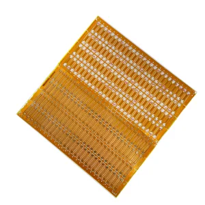
In the landscape of modern hardware manufacturing, standard printed circuit boards with 1oz (35µm) copper foil are no longer sufficient to handle the extreme electrical loads and thermal demands of advanced power electronics. Thick copper PCBs (commonly defined as boards featuring copper weights ranging from 3oz/sq.ft to over 20oz/sq.ft, or 105µm to 700µm) have emerged as the foundational architecture for efficient energy distribution. By utilizing heavy copper layers, design engineers can integrate high-current circuits and control signals onto a single, compact substrate, eliminating the need for bulky busbars, wire harnesses, or secondary heavy-gauge connectors.
This transition is primarily driven by the search for *optimal thermal management*. High current densities inherently generate resistive heat losses. The cross-sectional area of a thick copper trace dramatically lowers impedance, reduces heat dissipation requirements, and permits the safe transit of currents exceeding hundreds of amperes. Consequently, these robust architectures reduce the thermal stress on critical active devices, ensuring operational stability and mitigating board-level failures.
| Copper Weight (oz/sq ft) | Nominal Thickness (µm) | Recommended Min. Trace Width (mil) | Recommended Min. Spacing (mil) | Typical Applications |
|---|---|---|---|---|
| 3 oz | 105 µm | 8 mil | 10 mil | Industrial IoT Gateways, Power Supplies |
| 4 oz | 140 µm | 10 mil | 12 mil | EV On-board Chargers, Solar Converters |
| 6 oz | 210 µm | 15 mil | 18 mil | Heavy Machinery Control, EV Fast Chargers |
| 10 oz | 350 µm | 25 mil | 30 mil | Military Aerospace, High-Power Grid Inverters |
| 15+ oz | 525+ µm | 40 mil | 50 mil | Railway Traction, Heavy Industrial Distribution |
Portugal is positioning itself as a central hub for industrial innovation and clean energy deployment within Western Europe. Key geographic regions are witnessing a rapid shift toward advanced hardware systems, demanding reliable domestic and global supply lines for specialized components like thick copper PCBs.
The Autoeuropa cluster and surrounding sub-tier suppliers in the Setúbal district require heavy-duty electronic systems capable of withstanding the high thermal stress in automotive powertrains and chassis subsystems.
Portugal’s nationwide EV charging network (Mobi.E) requires fast-charging stations designed around heavy copper circuits to support rapid, high-power DC charging without safety risks.
With wind and solar plants providing a significant share of the national grid's energy, reliable power converters and inverters depend on thick copper substrates to ensure continuous grid stability.
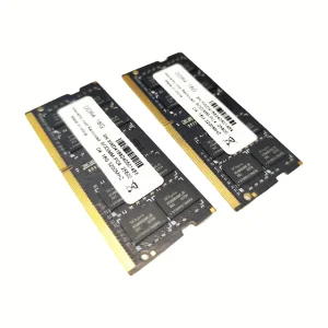
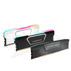
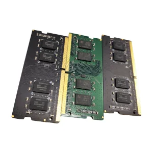
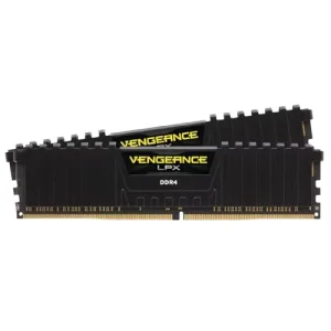
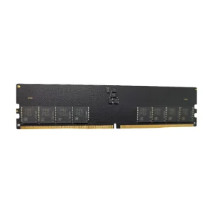
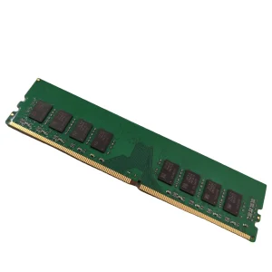
Additionally, the high-tech clusters in Aveiro and Porto are driving innovation in telecommunications, IoT, and embedded computing. In these ecosystems, combining heavy-duty power lines with high-speed control traces—such as those integrated with advanced DDR5 and DDR4 memory environments—is a standard approach to maximize power efficiency and computational performance in compact device footprints.
Fabricating boards with thick copper is not as straightforward as standard PCB assembly. The primary challenge lies in the isotropic nature of wet chemical etching. As the etchant eats downward into a heavy copper layer (e.g., 6oz), it also attacks the sides of the traces, causing an effect known as "undercutting." Fabricators must adjust the photolithographic artwork by applying a precise "etch compensation factor" to ensure the trace retains its required final width.
Furthermore, the high profiles of thick copper traces present challenges for solder mask application. Standard liquid photoimageable (LPI) solder masks can experience thin coverage on the upper corners of thick traces. To prevent exposure and subsequent electrical shorting, advanced manufacturers utilize multi-pass screen printing or electrostatically sprayed LPI masks, ensuring a uniform coating thickness of at least 0.8 mil over the corners of all conductors.
Leveraging 9 years of manufacturing excellence, specialized thermal management systems, and high-performance server memory solutions.
Established in 2016 in Shenzhen, China, Novram Electronics Co., Ltd. has grown to become a reliable supplier of high-speed memory modules, advanced thermal cooling sinks, and complex PCB assembly configurations. Operating from a modern 3,860㎡ manufacturing facility, we integrate automated production machinery with stringent quality management controls to serve partners in industrial automation, smart grids, and enterprise computing.
With 9 years of manufacturing expertise and 7 years of global export experience across 40 countries, Novram maintains an annual export revenue of approximately US$18.6 million. Our robust production ecosystem is supported by over 860 qualified supply chain partners, enabling consistent material sourcing and fast lead times for our global OEM, ODM, and industrial clients.
High-power industrial projects in Portugal require high reliability, and we ensure that quality remains at the center of our manufacturing workflow. Every product undergoes 100% functional testing, compatibility checks, burn-in verification, high-low temperature cyclings, and aging tests before dispatch. Our dedicated quality control division, consisting of 42 professional inspectors, ensures compliance with IPC standards and international electronics benchmarks.
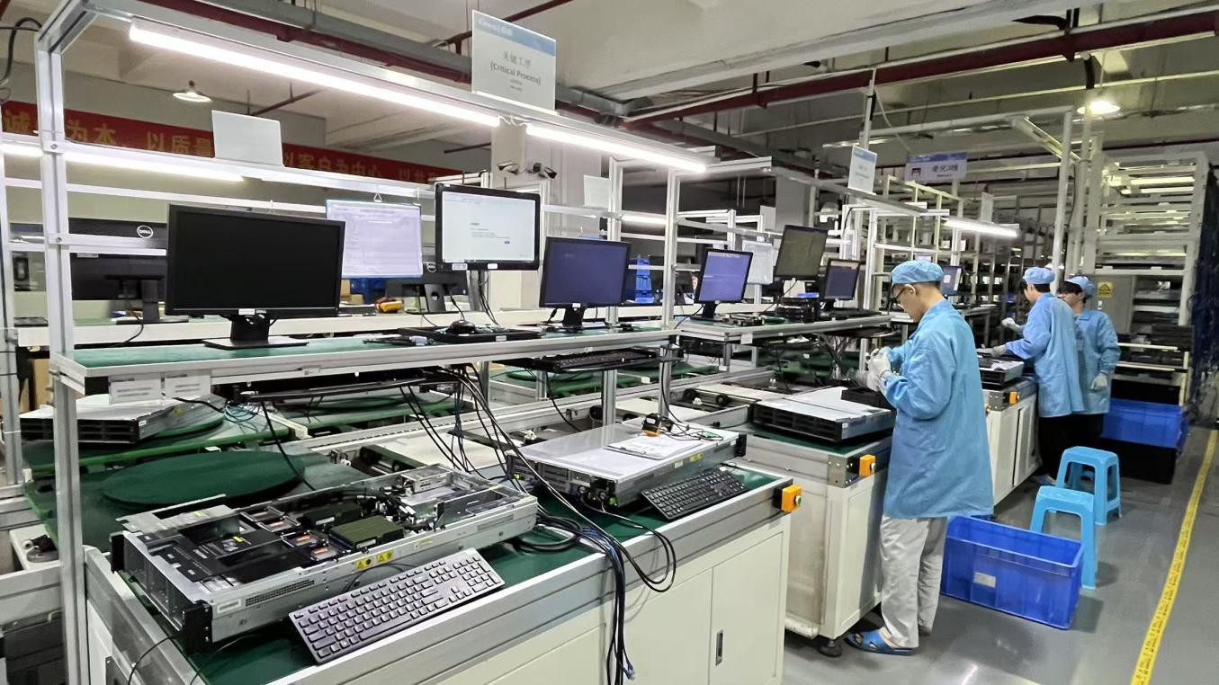

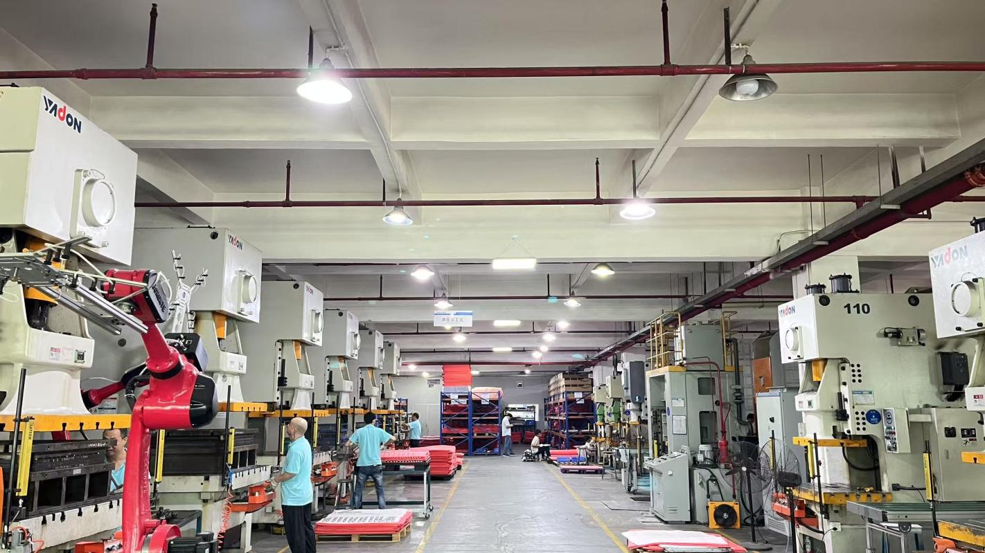
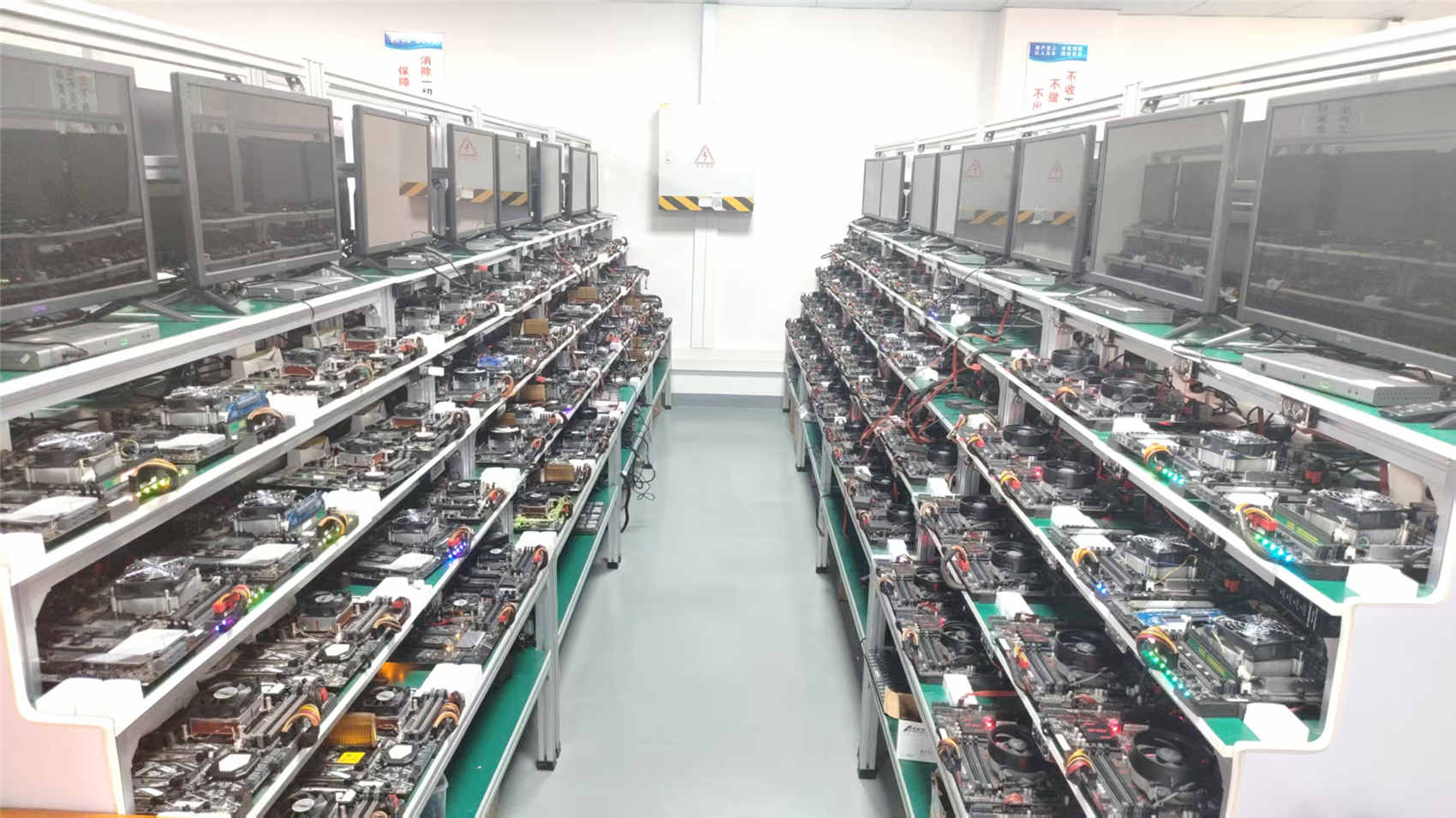
In the high-power electronics sector, managing lead times and material costs is crucial. China's Factory 4.0 infrastructure combines automated fabrication lines with mature component ecosystems to address these concerns:
Get answers to common design, manufacturing, and logistical questions regarding thick copper electronics.
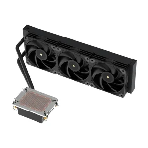
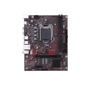
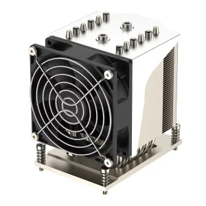
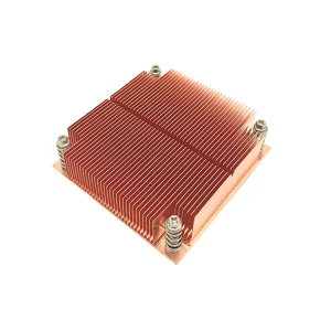
Explore our complete product catalog, featuring motherboards, heat sinks, and server-grade memory modules optimized for industrial use.