 Novram
Novram
Novram
Explore our high-performance manufacturing pipeline, producing high-reliability components engineered for Japan's demanding quality frameworks.
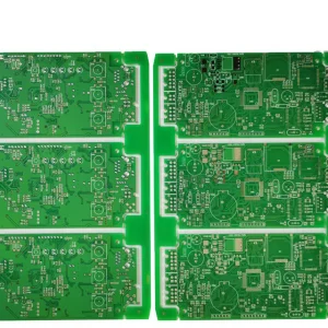
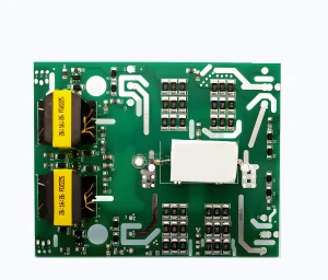
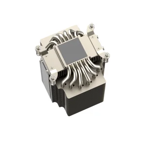
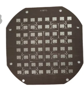
The Japanese industrial and consumer markets are leading a rapid transition from conventional mercury vapor lamps to UVC LED solid-state systems. Propelled by the Minamata Convention on Mercury and strict decarbonization mandates from the Ministry of Economy, Trade and Industry (METI), Japanese OEMs demand extremely durable, energy-efficient, and non-hazardous disinfection solutions.
Japanese markets operate under distinct technological expectations. Key application areas include municipal water purification plants, HVAC systems in high-density office high-rises across Tokyo and Osaka, and integrated clean-room sterilizers for the advanced semiconductor manufacturing sectors. For these highly critical use cases, standard commercial off-the-shelf LED modules often fall short. They require precision thermal interfaces and specialized driving circuitry to maintain optical efficiency and avoid catastrophic failures.
To address this complex landscape, our engineering capabilities bridge the gap between heavy-duty electrical components (like heat sinks, power drivers, and multi-layer PCBs) and high-performance optoelectronic demands. Our products are optimized to ensure minimal drop in optical power (L70 lifetime > 20,000 hours) under challenging operating environments.
We configure our manufacturing and processing structures to directly align with the Japanese Industrial Standards (JIS). Our production incorporates lead-free processing, halogen-free substrates, and compliant thermal materials to simplify import registration and VCCI/PSE safety audits for Japanese systems integrators.
UVC LEDs typically convert only 3% to 5% of electric energy into ultraviolet light, generating substantial heat. Our high-conductivity aluminum PCBs, high-reliability server memory modules for smart IoT edge controllers, and custom driver boards are optimized to maintain critical junction temperatures below 60°C.
Industry Experience
Dedicated R&D Center
QA & Reliability Control
New Products Annually
How advanced chip materials, custom packaging architectures, and smart controls drive efficiency in the Japanese ultraviolet disinfection sector.
Improving internal quantum efficiency (IQE) remains a core milestone. Advanced physical vapor transport (PVT) growth of bulk AlN (Aluminum Nitride) substrates provides lower defect density, achieving deep-ultraviolet emissions between 260nm and 280nm with exceptionally high optical output power.
To withstand intense UV radiation, standard epoxy-based packaging is replaced with High-Temperature Co-fired Ceramic (HTCC) substrates and fused silica glass lenses. This airtight, organic-free package design prevents degradation and yellowing under long-term exposure.
By deploying high-density memory modules (DDR4/DDR5) and smart IGBT drivers into monitoring control units, systems can dynamically sense temperature fluctuations and adjust forward currents, preventing thermal runaways while communicating module status to centralized controllers.
| Technology Generation | Wavelength Range (nm) | Primary Substrate Material | Thermal Management Need | Target Applications (Japan Market) |
|---|---|---|---|---|
| Standard UVC | 265nm – 280nm | Sapphire Substrates | High (requires Metal Core SMT) | Static Water Sterilizers, Home Air Purifiers |
| High-Flux UVC | 260nm – 275nm | Bulk AlN (Aluminum Nitride) | Critical (Requires Active Liquid Cooling) | Municipal Waste Water, Semiconductor Clean Rooms |
| Far-UVC | 222nm | Excimer / KrCl Filters & GaN | Moderate to High | Occupied Space Disinfection, Hospitals, Transit |
Novram Electronics Co., Ltd. is a professional electronics and hardware systems manufacturer based in Shenzhen, China, dedicated to delivering high-performance DRAM solutions, advanced thermal management components, and customized circuit board systems for global OEM, ODM, and industrial customers. Established in 2016, the company has grown into a highly reliable supplier, serving partners across consumer electronics, industrial automation, clean technology, embedded systems, and enterprise computing.
Operating from a modern, state-of-the-art 3,860㎡ manufacturing facility, Novram integrates advanced production equipment, strict quality management frameworks, and continuous R&D innovation. This infrastructure ensures that every memory module, power driver board, and thermal substrate meets international performance and reliability standards. Our experienced engineering team focuses on developing high-speed, stable, and energy-efficient products designed to operate under harsh industrial environments.
With 9 years of industry experience and 7 years of export experience, Novram exports products to customers in more than 40 countries, with a specialized service pipeline targeting the precise needs of industrial buyers in Japan. The company achieves an annual export revenue of approximately US$18.6 million, supported by an efficient global supply chain and responsive customer service portals.
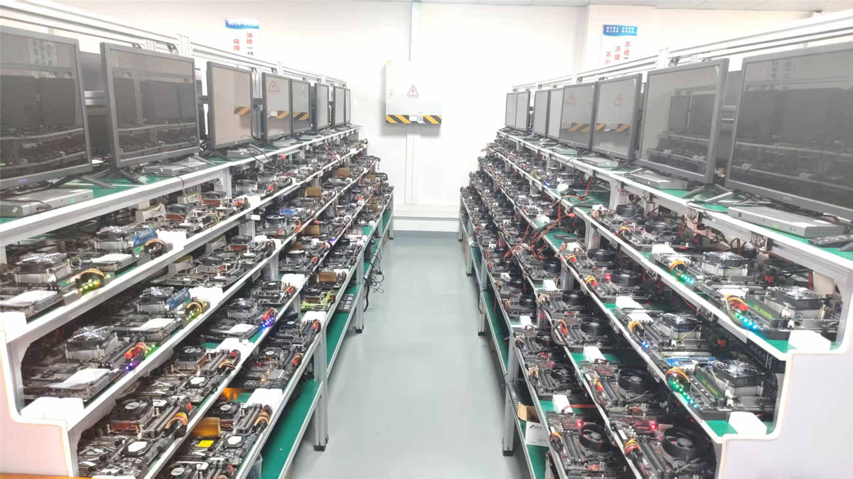
Quality is at the core of everything we do. Every component and sub-assembly undergoes 100% functional testing, compatibility testing, burn-in testing, temperature testing, and aging verification before shipment. Our quality control department consists of 42 professional inspectors, ensuring consistent product performance and long-term reliability.
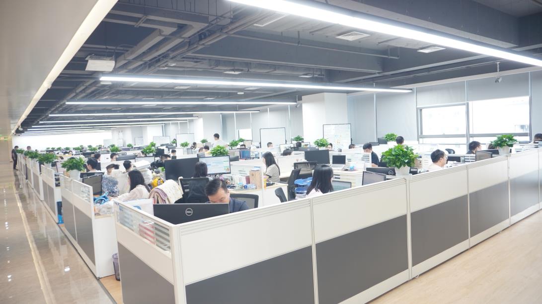
Novram maintains strong partnerships with over 860 qualified supply chain partners, enabling stable production capacity and reliable raw component sourcing. Our primary customers include memory module brands, computer manufacturers, industrial PC companies, system integrators, clean-tech distributors, and OEM/ODM partners worldwide. Innovation drives our competitiveness. Our dedicated R&D center is staffed by 76 experienced engineers, allowing us to introduce approximately 138 new products each year. We provide comprehensive OEM, ODM, private label packaging, capacity customization, firmware optimization, and product specification customization to meet different market requirements.
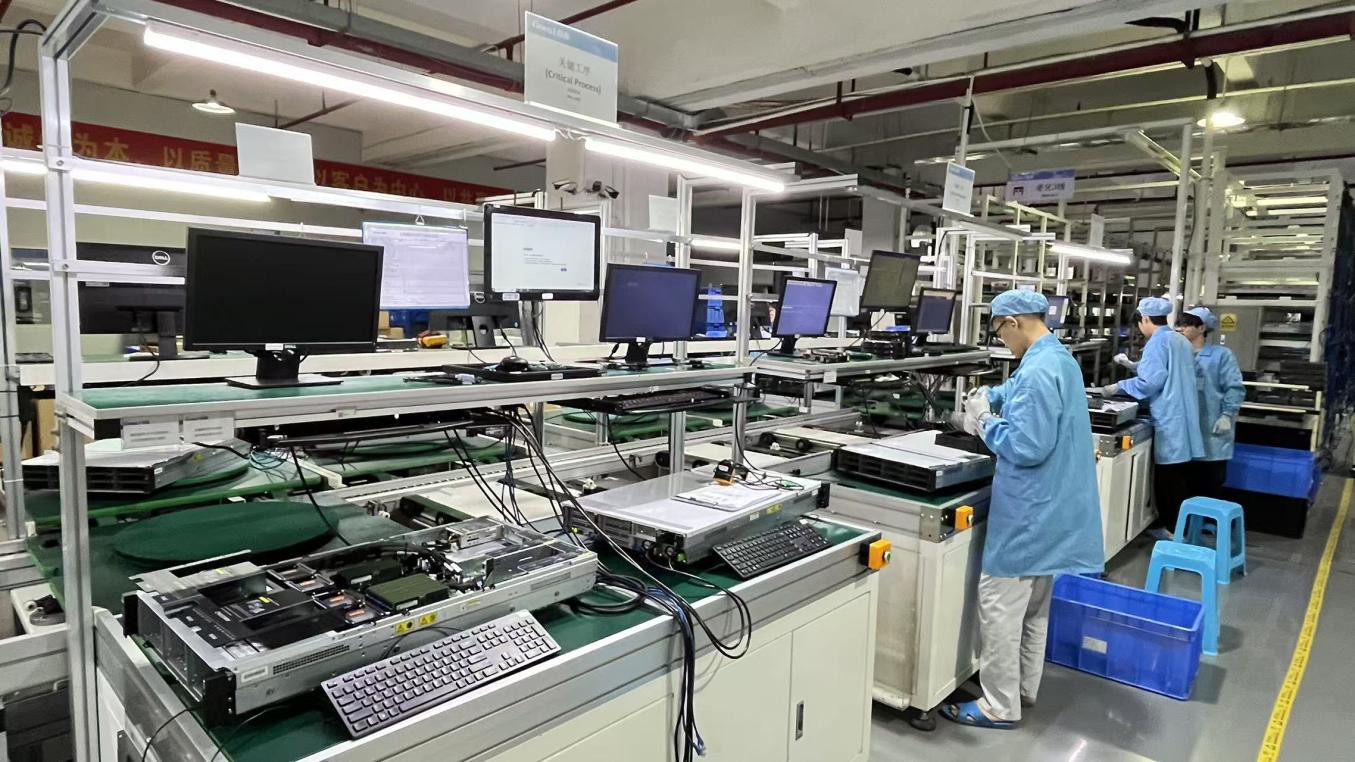
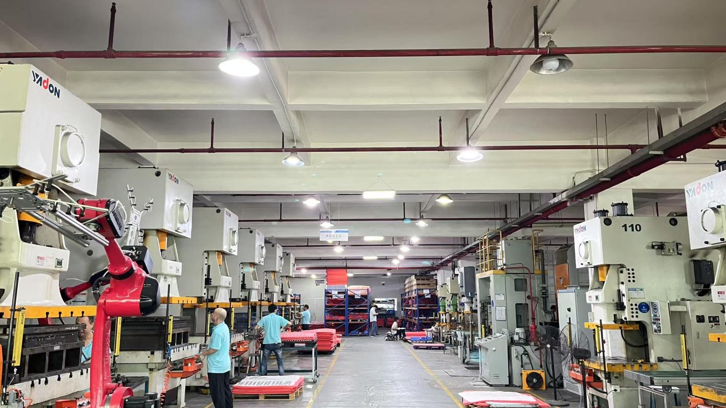
Our production facilities utilize modern high-speed SMT placement machines capable of handling high-power ceramic LED packages alongside integrated passive components. Copper-backed and aluminum-backed PCB lamination technologies provide optimized thermal conduction properties required for reliable disinfection modules.
To guarantee peak quality for Japanese clients, we employ automated optical inspection (AOI) alongside automated spectral testing of UVC wavelength distributions. Every batch is subjected to rigorous high-temperature aging chambers to screen out early component failures before packing.
By leveraging our strategic location in Shenzhen, the silicon hub of advanced manufacturing, we provide unparalleled supply chain resilience and cost efficiency. Our close integration with 860+ qualified suppliers allows us to secure premium components, copper substrates, high-performance thermal interfaces, and custom driver integrated circuits (ICs) with zero production delay.
For Japanese electronics companies, sourcing from our Shenzhen Factory 4.0 setup means access to advanced economies of scale without sacrificing quality metrics. We bridge localized supply chain advantages with top-tier international standardizations like ISO 9001:2015, ensuring a seamless flow of sub-assemblies to ports across Tokyo, Osaka, and Nagoya.
Through our dedicated design and testing capabilities, we support custom spectrum configurations, flexible substrate dimension designs, and variable driver footprints to ensure your UVC modules plug directly into existing hardware layouts.
How we align our design, manufacturing, and logistic workflows to match the precise expectations of Japan's technology sector.
All modules and circuit sub-assemblies are fully lead-free, conforming to standard RoHS and REACH environmental guidelines. We maintain trace reports on all chemical compositions, assisting your green procurement audits.
Our driver boards and power modules are manufactured with spacing, isolation, and dielectric characteristics that facilitate Denan (PSE) safety checks for integrated Japanese appliances.
With 7 years of deep export experience, we manage streamlined customs logistics directly to Tokyo (TYO), Osaka (OSA), Yokohama (YOK), and Kobe (UKB), including all origin documentation and duty certificates.
Integrating high-stability RAM modules, custom heat sinks, and PCB solutions for comprehensive hardware controllers used in disinfection networks.
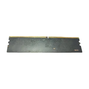
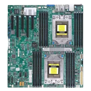
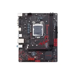
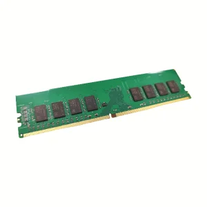
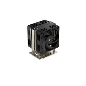
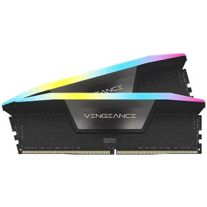
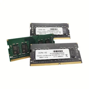
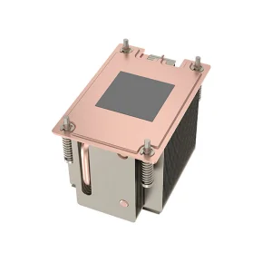
Ensuring the original product catalogue is fully preserved while offering modular versatility for industrial buyers.
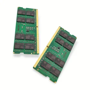
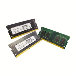
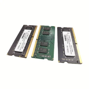
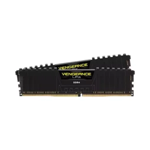
Understanding critical parameters, lead times, and engineering parameters before initiating a custom UVC LED sub-assembly production run.
UVC chip lifetime is inversely proportional to junction temperature. Buyers must evaluate the thermal dissipation path: junction-to-substrate, substrate-to-heat sink, and heat sink-to-ambient. Using high thermal conductivity materials like copper-filled vias or aluminum substrates is necessary to prevent thermal degradation.
UVC LEDs are current-driven devices with a steep forward voltage curve. Minor voltage fluctuations can cause large shifts in forward current, resulting in accelerated aging or burnout. Constant-current driver designs with built-in thermal feedback loops are highly recommended.
Ensure that procurement requests specify the expected optical output density at a given distance rather than simply listing raw electrical power wattage. For instance, air purifiers and surface sterilizers require precise irradiance patterns to achieve the necessary log-reduction values for targeted biological pathogens.
Step 1: Engineering Assessment — Share your dimensions, spectrum demands (e.g., 265nm, 275nm, or 222nm), and operating conditions.
Step 2: Circuit & Thermal Modeling — Our 76-engineer team models heat dissipation parameters and maps SMT routing layouts.
Step 3: Rapid Prototyping — Samples are produced and put through 100-hour continuous burn-in verification.
Step 4: Mass Custom Production — Scaled assembly in our 3,860㎡ factory, supervised by 42 QA inspectors.
Step 5: Direct Export — Fast freight dispatch with tracking to Japanese entry ports.
Find answers to technical and logistical queries concerning UVC module fabrication and delivery to Japan.
We primarily specialize in the germicidal 265nm to 275nm spectrum, which matches the peak absorption spectrum of DNA and RNA. Additionally, we support custom fabrication of 222nm Far-UVC filtering configurations and 310nm UVB modules for agricultural lighting applications.
We address thermal dissipation by implementing metal-core printed circuit boards (MCPCBs) using high-conductivity aluminum or specialized copper substrates. We also design customized active water cooling blocks and fan-assisted aluminum heat sinks to ensure junction temperatures remain low, extending component lifetime.
Standard design and prototype production take approximately 7 to 10 working days. Once confirmed by the client, mass manufacturing runs are scheduled, with standard ocean freight to major Japanese ports taking 5 to 7 days, and air express taking 2 to 3 days.
Yes. Our electronics assembly factory manufactures smart driver boards incorporating PWM dimming, temperature sensor feedbacks, and wireless communications, which are ideal for integration into smart factory controllers, remote monitoring units, and localized automation rigs.
Connect directly with our engineering team to request sample runs, technical drawings, or volume pricing for UVC components and controllers.